
PCB Manufacturing
PCB Manufacturing – Prototype to Mass Production
One-Stop Solutions for Rigid, Flexible, Rigid-Flex, HDI, and High-Speed PCBs
As a ISO9001:2015 and UL 94V-0 certified PCB manufacturer, we provide end-to-end PCB manufacturing services – from prototype validation to high-volume production. Unlike fab-only shops that focus solely on fabrication, we offer complete solutions including PCB fabrication, assembly, testing, and box build.
Whether you need standard FR4 boards, high-density HDI, flexible circuits, or ceramic substrates, we deliver consistent quality, competitive pricing, and reliable lead times – all under one roof.
One supplier. One quality standard. One point of contact. From prototype to production.
Why Choose Our PCB Manufacturing?
ISO9001 & UL Certified
Documented quality management system. Full traceability.
Prototype to Mass Production
Seamless transition – no supplier switching. Same quality, same process, same team.
Competitive China Pricing
Lower manufacturing costs without compromising quality.
Turnkey Assembly Available
PCB fabrication + component sourcing + SMT assembly + testing – one stop.
Strict Quality Control
100% AOI, 100% electrical test, X-Ray for BGA, IQC/OQC.
Full IP Protection
NDA available. Secure file handling. Your design stays yours.
Our PCB Fabrication Services
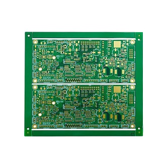
FR4 PCB
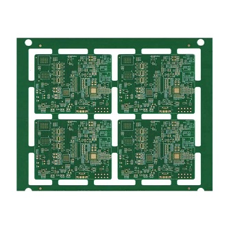
HDI PCB
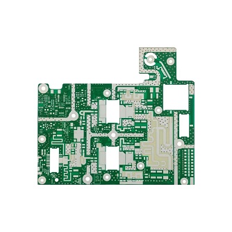
High-Frequency PCB
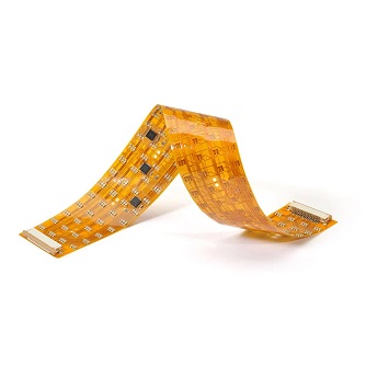
Flexible PCB
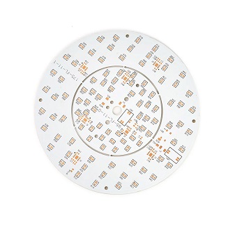
Aluminum PCB
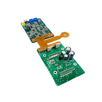
Rigid Flex PCB
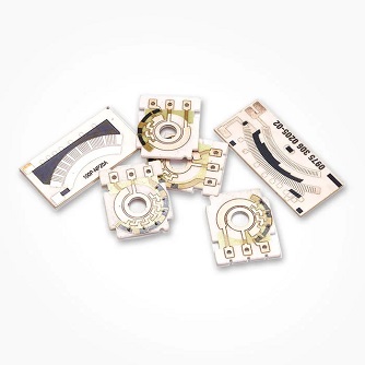
Ceram PCB
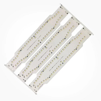
LED PCB
Our PCB Manufacturing Capabilities
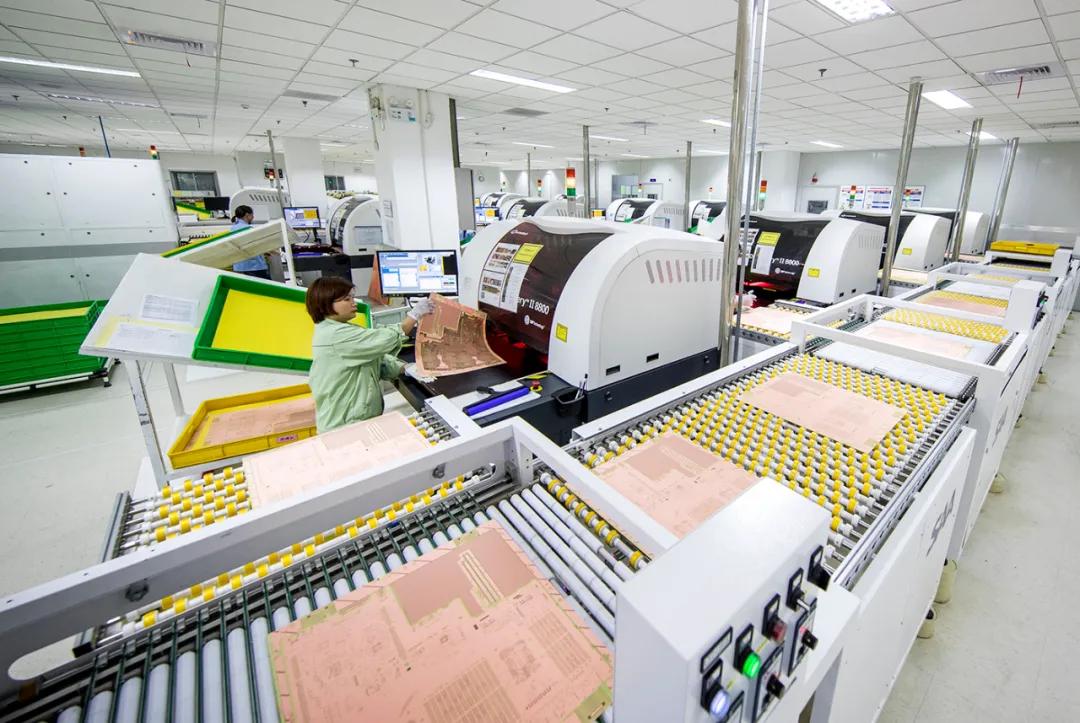
Layer count:1 to 12 layers(higher on request)
Board thickness:0.4mm to 3.2mm
Copper weight:0.5 oz to 6 oz
Min trace width/spacing:3 mil/3 mil(0.075mm)- HDI:2 mil available
Min drill size:0.15mm mechanical,0.10mm laser microvia
Surface finishes:ENIG,HASL Lead-Free,OSP,Immersion Silver,Immersion Tin,Hard Gold
Solder mask colors:Green,Blue,Red,Black,White,Yellow,Purple,Matt colors
Special capabilities:Controlled impedance,heavy copper,blind/buried vias,via-in-pad
Manufacturing & Quality Control Process
1.Material receiving:Incoming material inspection(IQC) - copper foil,prepreg,laminate
2.Inner layer imaging:AOI after etching - catches opens/shorts
3.Lamination:Temperature/pressure monitoring - prevents voids
4.Drilling:Automated drill - depth control for blind vias
5.Plating:Thickness measurement - ensures copper fill
6.Outer layer imaging:AOI - verifies trace integrity
7.Solder mask/Coverlay:Visual inspection - alignment,coverage
8.Surface finish:Thickness testing - ENIG,HASL,OSP
9.Electrical test:100% flying probe or fixture test - every board
10.Final inspection:OQC - dimension,appearance,packaging
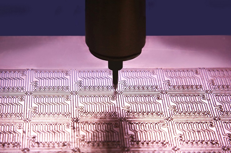
Ready to Start Your PCB Manufacturing Project?
👉Get a quick quote within 24 hours.
Upload your Gerber files and specifications. Our engineering team will review your design and provide a competitive quotation for prototype or production quantities.
✔ NDA Available ✔ Fast Quotation Within 24 Hours ✔ ISO Certified Factory ✔ One-stop PCB & PCBA Service