
What Is a Multilayer PCB?
A multilayer PCB is a type of printed circuit board that consists of three or more conductive copper layers stacked and laminated together with insulating materials in between. The outer layers function like a standard double-sided PCB, while the inner layers are used for routing signals, power, and ground planes.
These layers are electrically connected through plated vias (copper-coated holes), allowing signals to pass between layers. Depending on the application, a multilayer PCB can have up to 60 layers or more, enabling very high circuit density and advanced electrical performance.
Compared to single-sided or double-sided PCBs, multilayer boards support tighter component placement, shorter signal paths, and better power distribution, making them ideal for compact and high-performance electronic products.

Why Multilayer PCBs Are Essential in Modern Electronics
Printed circuit boards form the backbone of virtually every electronic system—from smartphones and medical devices to automotive electronics and aerospace equipment. A PCB consists of an insulating base material, typically fiberglass (FR-4), with conductive copper traces that electrically connect components.
While single-layer PCBs are still used for simple designs, modern electronics require smaller, faster, and more complex circuits. Multilayer PCBs make this possible by stacking routing layers vertically, allowing engineers to design high-density, high-speed, and highly reliable systems.
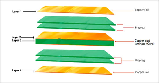
Anatomy of a Multilayer PCB
Unlike single-layer boards, multilayer PCBs use vias to connect copper layers together. These tiny conductive holes allow signals and power to travel between layers.
A typical multilayer PCB is made of:
Copper layers for signal, power, and ground routing
Dielectric laminates to electrically isolate layers
Prepreg bonding layers to laminate the stack
Solder mask for protection
Silkscreen for labeling
This precision-built structure ensures electrical stability, mechanical strength, and long-term reliability.
Anatomy of a Multilayer PCB
Advantages of Multilayer PCBs
High Circuit Density
Multiple layers allow more traces and components to fit into a smaller area, enabling compact and lightweight designs.
Improved Signal Integrity
Dedicated power and ground planes reduce noise, crosstalk, and EMI, ensuring stable high-speed signal transmission.
Better EMI Control
The stacked structure provides natural shielding, minimizing electromagnetic interference between signals.
Enhanced Reliability
Shorter signal paths and well-controlled power distribution improve overall system stability and performance.
Applications of Multilayer PCBs
Multilayer PCBs are used across a wide range of industries, including:
Telecommunications – 5G infrastructure, routers, and high-speed networking
Automotive electronics – ADAS, infotainment, and power control modules
Medical devices – imaging systems, monitoring equipment, and diagnostic tools
Aerospace and defense – avionics, navigation, and mission-critical electronics
Industrial automation – control systems and embedded computing
Design and Manufacturing Challenges
Designing a multilayer PCB requires careful control of:
Signal integrity and impedance
Power distribution and grounding
Thermal management
Layer alignment and via structure
Advanced PCB design tools and strict manufacturing processes are required to ensure that all layers are precisely aligned and electrically reliable.
Conclusion
Multilayer PCBs are a cornerstone of modern electronics. By delivering high performance, compact size, and excellent reliability, they enable the advanced devices we rely on every day—from medical equipment to next-generation communication systems.
If you are looking for a reliable PCB and PCBA partner, Tengxinjie provides complete solutions including PCB design, PCB fabrication, PCB assembly, and testing, helping you bring complex electronic products to market faster and with confidence.