 PCB & PCBA Manufacturer

In modern electronics, the performance and long-term reliability of a finished product are directly tied to the quality of its Printed Circuit Board Assembly (PCBA) . Even minor defects at the board level—such as microscopic solder cracks, misaligned components, or incorrect passive values—can escalate into costly field failures, product recalls, and lasting damage to a brand’s reputation.
High-quality PCBA is not achieved through a single final inspection. It is the result of a systematic, multi-stage testing workflow that begins before the first reel of components is loaded and continues until every assembled board has demonstrated full functionality.
For complex, high-density designs, partnering with a manufacturer that implements advanced inspection and test methods is essential. At Tengxinjie, we integrate rigorous, technology-driven PCBA inspection throughout the entire assembly process to ensure every board meets the highest standards of performance and reliability.
This guide outlines best practices and advanced techniques used in a professional PCBA testing workflow—from component verification to final functional testing.
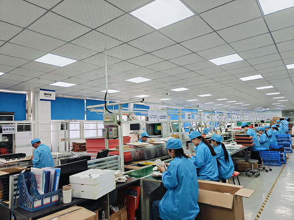
1. PCBA Testing: Pre-Assembly Verification
The most effective way to prevent defects is to ensure that only verified components and PCBs enter the assembly line. This foundational stage, known as Incoming Quality Control (IQC) , is the critical first line of defense.
1.1 Incoming Quality Control (IQC) for Components
Every PCBA begins with a Bill of Materials (BOM). The integrity of the final product depends on the absolute accuracy of the components used. IQC for components is a comprehensive verification process that includes:
Authenticity and Part Number Verification: Components are validated against the BOM and manufacturer datasheets to confirm part numbers, values (resistance, capacitance), and tolerances. This step is vital to eliminate counterfeit or incorrect parts that could cause immediate or latent failures.
Moisture Sensitivity Level (MSL) Management: Many ICs and passive components are hygroscopic—they absorb moisture from the air. Each component has an MSL rating, which defines its allowable “floor life” outside dry storage. During reflow soldering, trapped moisture vaporizes, creating internal pressure that can cause delamination, bond wire failure, or “popcorning.” Proper IQC includes verifying MSL ratings, checking dry pack seals, and baking components that have exceeded their floor life.
Tengxinjie offers in-stock component sourcing with rigorous verification processes, minimizing the risk of counterfeit or incorrect parts. We expertly manage MSL components through careful storage, tracking, and handling protocols.
1.2 Bare PCB Inspection
The bare PCB itself is a complex engineered product. Before it enters the SMT line, it must undergo its own set of quality control checks:
Visual and Automated Optical Inspection (AOI): Each board is inspected for surface defects such as scratches, contamination, or pad oxidation. AOI systems also verify that trace widths and spacing comply with design rules.
Dimensional Checks: Critical dimensions, board thickness, and plated through-hole (PTH) diameters are measured to ensure mechanical compatibility and proper component fit. Warpage and twist are also measured, as excessive bowing can cause problems during solder paste printing and component placement.
Electrical Testing (E-Test): This is arguably the most critical PCB test. Using a “bed-of-nails” fixture for high-volume runs or a “flying probe” tester for prototypes, E-Test confirms connectivity—ensuring that nets that should be connected are connected, and that separate nets are not shorted together.
Solder Mask and Silkscreen Registration: The alignment of solder mask and silkscreen layers is verified. Misaligned solder mask can lead to solder bridging; misaligned silkscreen can cover pads or cause incorrect component placement during manual assembly or rework.
| Defect Type | Potential Impact | Primary Detection Method |
|---|---|---|
| Counterfeit IC | Complete or intermittent functional failure, reduced lifespan | Supplier verification, XRF, decapsulation |
| Incorrect Component Value | Circuit malfunction, damage to other components | Part number verification, LCR measurement during IQC |
| Component Oxidation | Poor solderability, weak or non-existent solder joints | Visual inspection, solderability testing |
| Excessive PCB Warpage | Poor solder paste stencil seal, placement issues | Measurement per IPC-A-600 |
| PCB Internal Short/Open | Complete functional failure of affected circuit | Electrical Testing (E-Test) |
2. PCBA Testing: In-Process Inspection
Once materials are verified, inspection becomes an integral part of the SMT assembly line. These in-process inspections enable real-time feedback to identify defects at their source.
2.1 Solder Paste Inspection (SPI)
Industry data consistently shows that 60-70% of all SMT defects can be traced back to the solder paste printing process. Therefore, inspecting solder paste deposits before component placement is one of the highest-value inspection steps.
Modern manufacturing relies on 3D SPI machines, which use laser triangulation to create a topographical map of the solder paste on every pad. Unlike older 2D systems that only checked area and bridging, 3D SPI provides precise quantitative data on:
Volume: Total amount of solder paste—enough for a strong joint but not so much as to risk bridging.
Height: Critical for ensuring components will sit correctly in the paste.
Area: Coverage of paste on the pad.
XY-Offset: Alignment of the paste deposit on the pad.
This data allows immediate process correction. For example, if the machine detects a gradual decrease in paste volume, it may indicate a clogged stencil aperture.
2.2 Automated Optical Inspection (AOI)
AOI systems use high-definition cameras and advanced image analysis software to autonomously scan PCBA assemblies for defects. AOI is typically employed at two key points:
Pre-reflow: Checks for correct component placement, presence/absence, orientation (diodes, capacitors, ICs), and ensures tombstoning has not occurred before reflow. Finding defects at this stage makes rework significantly easier.
Post-reflow: This is the most common application. AOI inspects solder joint quality, looking for solder bridges, insufficient solder, excess solder, and lifted leads.
Limitation: While AOI is extremely effective for surface defects, it cannot see hidden features. It is not applicable for inspecting solder joints under components such as BGAs and QFNs.
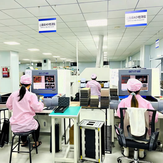
AOI and X-Ray PCB Inspection in PCB Assembly
2.3 Automated X-Ray Inspection (AXI)
Automated X-Ray Inspection (AXI) is the industry standard for evaluating non-visible solder joints. AXI systems can image through IC packages—down to the silicon level—to reveal BGA solder balls, QFN thermal pads, and hidden leads. AXI is essential for:
Solder Joint Integrity: Detecting shorts, opens, and proper joint formation.
Void Detection: Identifying gas bubbles trapped inside solder joints. Excessive voiding can compromise thermal and electrical performance and increase mechanical failure risk.
Component Alignment: Verifying BGA ball pattern alignment to PCB pads.
Advanced 3D AXI systems can digitally slice through the board, isolating and inspecting individual layers on densely populated, double-sided assemblies.
3. PCBA Testing: Final Electrical & Functional Validation
Once a board is fully assembled, the final inspection phase focuses on overall quality and function.
3.1 Visual Inspection and IPC Standards
While automated systems are advanced, a trained human inspector remains invaluable. Technicians perform final visual checks, looking for subtle defects that machines might miss.
This inspection is governed by rigorous standards aligned with global industry benchmarks—primarily IPC-A-610, “Acceptability of Electronic Assemblies.” This document provides the visual “rulebook” for acceptable solder joints, component placement, and assembly quality. It defines three product classes:
Class 1: General Electronic Products (e.g., consumer toys)
Class 2: Dedicated Service Electronic Products (e.g., laptops, smartphones)
Class 3: High-Performance/Harsh Environment Products (e.g., medical life support, aerospace, automotive)
| Feature | Class 1 (Target) | Class 2 (Acceptable) | Class 3 (Acceptable) |
|---|---|---|---|
| End Joint Width | Width (W) ≥ 75% Lead (L) | W ≥ 50% L | W ≥ 75% L |
| Side Joint Length | Length (D) ≥ 3 x W | D ≥ 1.5 x W or 0.5mm | D ≥ 3 x W or 0.5mm |
| Solder Wetting | Well-wetted fillet visible | Wetting is evident | Well-wetted fillet visible |
Tengxinjie’s adherence to ISO 9001:2015 and IATF 16949:2016 ensures that visual inspection processes are documented, repeatable, and traceable.
3.2 Flying Probe Test (FPT)
The Flying Probe Test is ideal for prototypes and low-volume PCBA. It uses 2-6 robotic probes that move across the board, touching test points to verify shorts, opens, and component values (resistors, capacitors). This method offers high flexibility and eliminates the need for custom fixtures, though test time per board is slower compared to ICT.
3.3 Functional Testing (FCT)
Functional Testing is the ultimate “go/no-go” test. It simulates the PCBA’s final operating environment. Using a custom fixture or test bench, the board is powered and communications are established to validate its behavior against design specifications.
For example: Does the LED blink at the correct frequency? Is data being transmitted correctly by the wireless module? Are sensor readings accurate? FCT confirms that the entire system works as intended.
3.4 In-Circuit Testing (ICT)
In-Circuit Testing (ICT) is best suited for high-volume, mature products. It uses a custom “bed-of-nails” fixture to contact designated test points. The board is powered on, and each component is electrically tested individually to verify correct values, as well as shorts and opens. ICT delivers excellent fault coverage but has higher upfront fixture costs.
Conclusion
Ensuring robust PCBA quality is not a single action but a comprehensive, integrated strategy. From verifying components and bare boards before assembly, to using real-time SPI, AOI, and AXI data on the SMT line, to final inspections against IPC standards and functional requirements—each stage builds on the previous one.
This multi-layered approach is the only way to systematically eliminate defects, reduce field failures, and deliver the highest reliability in a final product.
Ready to verify and assure the quality of your next electronics project? Upload your files for a quick quote and take advantage of Tengxinjie’s advanced inspection processes today.
FAQs About PCBA Testing
Q1: What is PCBA testing?
PCBA testing is the process of inspecting, measuring, and validating assembled circuit boards to ensure they function correctly. It includes SPI, AOI, AXI, flying probe, ICT, and functional testing.
Q2: What are the main PCBA testing methods?
The main methods are:
Solder Paste Inspection (SPI)
Automated Optical Inspection (AOI)
Automated X-Ray Inspection (AXI)
Flying Probe Testing (FPT)
In-Circuit Testing (ICT)
Functional Testing (FCT)
Q3: What is the main difference between AOI and AXI?
AOI uses visible light to detect external, surface-level defects (incorrect placement, polarity errors, solder bridges). AXI uses X-ray imaging to inspect internal or hidden features—such as BGA solder balls, QFN thermal pads, and voids—that AOI cannot see.
Q4: Can Functional Testing (FCT) replace AOI or ICT?
No. FCT complements AOI and ICT but does not replace them. AOI/ICT detect manufacturing defects (opens, shorts, misplacements), while FCT verifies that the board performs its intended electrical and system functions. A robust quality workflow includes all three.
Q5: How does PCB complexity influence inspection method selection?
As complexity increases, inspection requirements become more advanced. Simple boards may only need manual visual checks and basic AOI. Dense, multilayer, or component-rich designs—especially those with BGAs, WLPs, or QFNs—require 3D SPI, 3D AOI, ICT, and AXI to properly verify solder joints and component integrity.
WeChat
Scan the QR Code with WeChat