PCBA Assembly & Electronics Manufacturing Services Provider

WiFi Module Sensor PCBA Solution - One-stop PCBA Solutions

Sensors & Actuators PCBA/Industrial Automation PCBA/


WIFI Module Sensor PCBA Solution

Application: Industrial Automation Solutions

Layers: 1-32

Material: FR-4

Thickness: 1.6 mm

Copper: 1 oz

Surface Finish: HASL

Model: TXJ-IASA-03

Use: WIFI Module Sensor

Related products:   Industrial Automation PCBA

  • Product Details
  • FAQs
  • Shipping & Delivery

Precision Engineering for WiFi Module Sensor PCBA

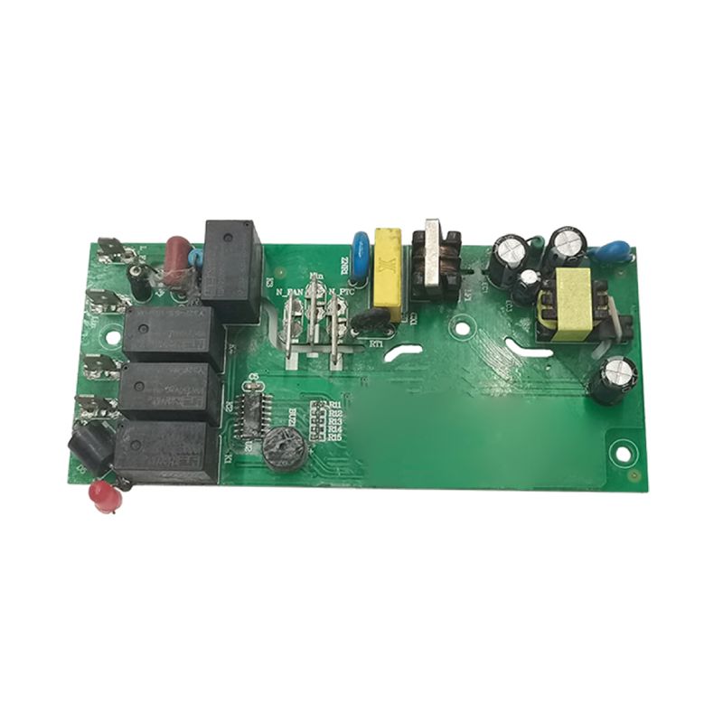
A wifi module sensor pcba is a high-complexity environment where analog sensor data must coexist with high-frequency digital signals. The primary challenge in wireless sensor design is maintaining signal integrity while preventing electromagnetic interference (EMI). Our engineering team specializes in the nuances of RF layout, ensuring that the antenna performance is optimized and that noise from power conversion circuits does not desensitize the WiFi receiver.

By choosing our specialized wifi module sensor pcb assembly services, you benefit from a partner who understands “Design for Excellence” (DFX). We perform a rigorous review of your schematics and board layout to ensure that impedance control is maintained on all high-speed traces. This meticulous approach to pcba manufacturing reduces the risk of costly redesigns and ensures your product passes international regulatory certifications, such as FCC, CE, and IC, on the first attempt.

Advanced WiFi Module Sensor SMT Board Assembly

The trend toward miniaturization in IoT means that sensors are becoming smaller while their processing power increases. This requires a sophisticated wifi module sensor smt board assembly process. Our facility is equipped with state-of-the-art SMT lines that feature high-precision placement heads capable of handling 01005 components and the fine-pitch LGA/QFN packages typically found in modern WiFi modules like the ESP32, Realtek, or Nordic series.

Our smt pcb assembly capabilities include:

  • 3D Solder Paste Inspection (SPI): Essential for wireless modules where even a minor solder bridge or insufficient paste can lead to intermittent RF failure.

  • Automated Optical Inspection (AOI): Post-reflow verification to ensure every component on your wifi module sensor smt board assembly is perfectly placed and soldered.

  • Nitrogen-Purged Reflow: To ensure the highest quality solder joints with minimal oxidation, which is critical for the long-term reliability of sensors operating in harsh environments.

Comprehensive Turnkey PCB Assembly Solutions

For B2B procurement managers, managing the global supply chain for electronic components can be a significant burden. Our wifi module sensor pcb assembly service is a full-turnkey solution. We manage the entire lifecycle—from sourcing long-lead-time WiFi chips and sensors from authorized distributors to the final functional testing of the completed board.

By integrating pcb assembly with our deep supply chain network, we provide:

  1. Authorized Component Sourcing: Zero-risk procurement of active and passive components.

  2. Impedance Control & RF Testing: We don’t just assemble; we can verify that the RF path meets your design specifications.

  3. Custom Functional Testing (FCT): We develop custom test jigs to verify the WiFi connectivity, sensor accuracy, and power consumption of every wifi module sensor pcba before it leaves our factory.

Why Quality PCBA Manufacturing is the Key to IoT Success

In the B2B sector, the cost of a field failure far outweighs the initial unit price. A sensor that loses connectivity or consumes its battery too quickly results in customer dissatisfaction and expensive warranty claims. That is why our pcba manufacturing process adheres to IPC-A-610 Class 2 and Class 3 standards.

We emphasize transparency and technical communication. Our Western clients value our ability to provide detailed DFM (Design for Manufacturing) reports that highlight potential yield issues before production begins. This collaborative approach to pcb assembly ensures that your wifi module sensor smt board assembly is optimized for both performance and cost-efficiency.

Scaling Your IoT Vision with a Reliable Partner

The demand for smart, connected sensors is growing across every industry, from medical healthcare to agriculture. To compete, you need a manufacturing partner that can scale with you—from small-batch NPI (New Product Introduction) prototypes to high-volume mass production.

Our expertise in smt pcb assembly and our dedicated focus on wireless technology make us the ideal choice for companies seeking a high-tier wifi module sensor pcb assembly partner. We combine the logistical advantages of China’s electronics ecosystem with the quality management and communication standards expected by the international business community.

Q: What is the standard ordering process for Tengxinjie’s PCBA manufacturing services?

A: PCB assembly steps:

  1. Submission of technical documents (Gerber files, BOM, pick-and-place, test requirements, etc.)
  2. Quotation review and lead-time confirmation
  3. Prototype build and customer approval (if required)
  4. Mass production with quality inspection (AOI, X-ray, functional testing)
  5. Final packaging and shipment
  6. After-sales technical support and feedback

This process ensures accuracy, traceability, and smooth transition from prototype to mass production.

Learn more: Tengxinjie Ordering Guide


Q: What Base Materials Does Tengxinjie Offer for PCB Manufacturing?

A: Tengxinjie offers a wide selection of PCB Base Materials, including standard FR4, HDI PCB, Flexible PCB, Rogers PCB, Teflon, copper-core, and aluminum substrates. With these options, you can easily select the most suitable material to ensure the best performance for your project.


Q: Does Tengxunjie accept small-batch or prototype orders?

A: Yes. We support small-batch production and prototype orders, typically with minimum order quantities ranging from 10 to 200 pieces.

However, small-batch production may result in higher unit costs, and certain electronic components have minimum order quantity (MOQ) requirements.
Partnering with a flexible PCBA supplier enables startups and R&D teams to advance product development without significant upfront investment.


Q: What is the typical PCBA lead time? What affects delivery time?

A: PCBA lead time depends on order size and project complexity. Typical estimates are:

  • Prototype builds: 5–10 working days

  • Small-batch production: 10–15 working days

  • Mass production: 15–30+ working days

Key factors that impact lead time include:

  • Component availability and specified brands

  • Turnkey service scope

  • PCB layer count and complexity

  • Testing and inspection requirements

An experienced PCBA manufacturer can help manage these factors to keep your project on schedule.


Q: How are PCBA boards packaged and shipped?

A: PCBA boards are packed according to their sensitivity and shipping method. Standard packaging includes:

  • ESD-safe anti-static bags

  • Bubble wrap, foam, or anti-static trays

  • Moisture-proof, labeled outer cartons with tracking information

For medical, automotive, or high-reliability electronics, cleanroom packaging or special handling is available.
Most PCBA suppliers support air freight, sea freight, and express courier based on order size and urgency.


Q: What are the advantages of turnkey PCBA and one-stop manufacturing?

A: Turnkey PCBA services mean the manufacturer handles everything — Electronic component sourcing, PCB fabrication, PCB assembly, testing, and logistics.

A reliable one-stop PCBA supplier helps customers:

  • Simplify supply chain management
  • Reduce sourcing and communication errors
  • Shorten production lead time
  • Speed up time-to-market

This is especially valuable for OEMs, startups, and engineering teams that need fast and stable production.


Q: How do we ensure the quality of electronic components used in assembly?

A: We maintain a rigorous supplier qualification process and a global procurement network, sourcing parts exclusively from authorized and trusted distributors. All incoming components undergo stringent inspection to verify authenticity and quality before being deployed.


Shipping Terms

Shipping costs are paid by the buyer.
We normally ship via DHL, UPS, FedEx, or TNT.
Alternatively, you may provide your own courier account or arrange delivery to your freight forwarder in China.

For large-volume orders, sea freight is available.


Delivery to Port (FOB Terms)

When shipping to a port, Tengxinjie is responsible for transporting the goods to the departure port.
All customs clearance, ocean freight, insurance, and onward transportation after that point are the responsibility of the buyer.

Tengxinjie can recommend reliable local freight forwarders upon request.
With the buyer’s authorization, Tengxinjie may also assist in coordinating shipping, with all related costs charged to the buyer.


Notice

The above shipping information is for reference only.
Tracking details and shipment updates will be provided once the order has been dispatched.

PCBA Shipping Delivery

PCBA Shipping Delivery

Prev:

Next:

Leave a Reply

Get a Quote ?

[contact-form-7 id="548" title="Contact Form"]