
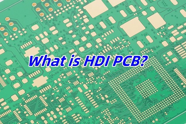
HDI PCB Design Guidelines
HDI PCB design has become essential for modern electronics such as smartphones, wearables, automotive systems, and IoT devices. With the demand for smaller, faster, and more powerful products, HDI technology plays a critical role in achieving compact layouts and high performance.
However, HDI pcb design also introduces complexity in fabrication and pcba manufacturing hdi, requiring careful planning to ensure manufacturability, reliability, and cost control. This guide covers the most important HDI PCB design guidelines to help you optimize your design for efficient smt pcb assembly and a reliable pcba service.
HDI PCB design
What Is an HDI PCB
HDI PCB design are characterized by higher wiring density per unit area compared to traditional boards. They typically include:
Microvias (laser-drilled vias)
Blind and buried vias
Fine lines and spacing
High layer counts with sequential lamination
These features allow designers to fit more functionality into smaller spaces, but they also increase the complexity of pcba manufacturing hdi and fabrication processes.
Stack-Up Planning Is Critical
A well-defined stack-up is the foundation of a successful HDI design.
Key considerations:
Determine the number of layers early
Plan sequential lamination cycles
Balance signal, power, and ground layers
Ensure symmetry to avoid warpage
Improper stack-up design can lead to signal integrity issues and higher fabrication costs, ultimately affecting your pcba service efficiency.
Collaborate with your manufacturer early to define a stack-up that is both functional and cost-effective.
Microvia Design Guidelines
Microvias are the core feature of HDI PCBs.
Best practices:
Use laser-drilled microvias for high precision
Keep aspect ratio ≤ 1:1
Limit microvia diameter (typically 75–150 µm)
Avoid excessive stacking of vias
Stacked microvias increase cost and reliability risks in pcba manufacturing hdi. Staggered vias are generally more reliable and cost-effective.
Proper microvia design improves yield and reduces defects during smt pcb assembly.
Via Structure Optimization
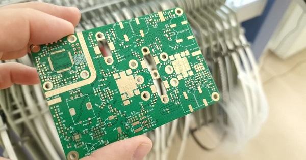
pcba manufacturing HDI
HDI designs often use a combination of:
Through-hole vias
Blind vias
Buried vias
Microvias
Guidelines:
Minimize via types to simplify fabrication
Avoid unnecessary via-in-pad unless required
If using via-in-pad, ensure proper filling and planarization
Via-in-pad is common for BGA components in smt pcb assembly, but it increases cost due to additional processing steps in pcba manufacturing.
Trace Width and Spacing
HDI PCBs require fine trace routing.
Typical guidelines:
Trace width: 50–75 µm (or smaller depending on capability)
Spacing: equal to or greater than trace width
Maintain consistent impedance for high-speed signals
Tighter spacing increases fabrication difficulty and cost. Always confirm your manufacturer’s capability before finalizing the design for pcba service.
Component Placement Strategy
Component placement is crucial in HDI design and directly affects smt pcb assembly efficiency.
Best practices:
Place high-pin-count ICs (e.g., BGAs) first
Group related components together
Minimize signal path length
Keep sensitive analog and high-speed digital circuits separated
Efficient placement reduces routing complexity and improves performance in pcba manufacturing.
BGA Fan-Out Design
Ball Grid Array (BGA) components are common in HDI PCBs.
Fan-out strategies:
Use microvias directly from pads
Apply via-in-pad for high-density BGAs
Optimize escape routing channels
Proper fan-out design ensures reliable connections and reduces assembly defects in smt pcb assembly.
Poor fan-out design can lead to routing congestion and increased layer count in pcba manufacturing.
Signal Integrity and Impedance Control
smt pcb assembly HDI
High-speed designs require strict signal integrity control.
Key considerations:
Controlled impedance traces
Differential pair routing
Minimized crosstalk
Proper grounding
Work with your manufacturer to define impedance requirements early to ensure consistency in both fabrication and pcba service.
Thermal Management
As density increases, thermal issues become more critical.
Solutions include:
Thermal vias under power components
Copper pours for heat dissipation
Proper component spacing
Effective thermal design improves reliability and prevents failures during pcba manufacturing and real-world operation.
DFM (Design for Manufacturability)
DFM is essential for reducing cost and improving yield in HDI projects.
Important DFM guidelines:
Follow manufacturer design rules
Avoid extreme tolerances unless necessary
Standardize materials and processes
Limit sequential lamination steps
A strong DFM approach ensures your design is compatible with efficient pcba service and scalable production.
DFT (Design for Testing)
Testing becomes more challenging in HDI pcb design due to high density.
Recommendations:
Add accessible test points
Avoid placing test points under components
Plan for ICT or functional testing early
Good DFT design improves test coverage and reduces debugging time in pcba manufacturing.
Material Selection
Material choice affects both performance and cost.
Common options:
FR4 for general applications
High-frequency materials for RF designs
Low-loss materials for high-speed signals
Choose materials based on actual requirements to avoid unnecessary cost increases in your pcba service.
Panelization Considerations

PCB high density design
Panelization is often overlooked but critical for smt pcb assembly.
Guidelines:
Use standard panel sizes
Ensure proper spacing between boards
Add fiducials for alignment
Include tooling holes
Good panel design improves production efficiency and reduces handling issues in pcba manufacturing.
Common HDI Design Mistakes to Avoid
Avoid these common errors:
Overusing stacked microvias
Ignoring manufacturer capabilities
Poor stack-up planning
Inadequate spacing for assembly
Missing impedance control requirements
These mistakes can lead to higher costs, delays, and lower yield in pcba service.
How to Balance Cost and Performance
HDI pcb design often involves trade-offs.
Cost optimization tips:
Use HDI only where necessary
Minimize layer count
Reduce via complexity
Standardize components
Balancing performance and manufacturability is key to successful pcba manufacturing.
Conclusion
HDI PCB design enables compact, high-performance electronic products, but it requires careful planning and adherence to strict guidelines. By optimizing stack-up, microvia design, component placement, and manufacturability, you can achieve reliable and cost-effective results.
In 2026, collaboration with your pcba service provider is more important than ever. A well-designed HDI board not only improves product performance but also ensures smooth smt pcb assembly and scalable pcba manufacturing.