
PCB Order Guidelines
These guidelines help ensure your PCB is manufactured correctly and without delays.
1. Solder Mask Bridges
To create solder mask bridges between pads or pins, the minimum spacing must be:
≥ 0.20 mm for 1–2 layer boards
≥ 0.10 mm for multilayer boards
You must clearly state “Solder mask bridge required” in the order remarks.
If not specified, the bridge may be removed during production.
2. Files Inside the ZIP Package
Only Gerber files are used for production.
All other files (PDF, DXF, Excel, notes, etc.) are ignored unless their information is included in the Gerber or mentioned in the order remarks.
Make sure:
All special requirements are reflected in the Gerber
Critical instructions are also written in the Remark field
3. PCB Files vs Gerber Files
If both PCB design files and Gerber files are included, Gerber files always take priority.
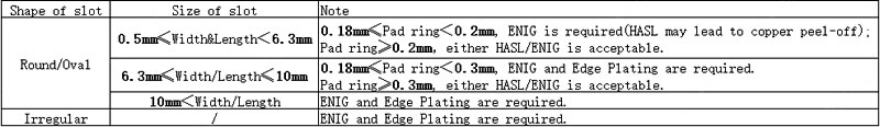
4. Plated Slots
Minimum requirements:
Minimum width: 0.5 mm
Length ≥ 2 × width
Square-cornered slots are not supported (corners must be rounded)
Edge Plating
To request edge plating:
Include its location in the Gerber
Mention it in the Remark field
We strongly recommend selecting Confirm Production File
5. Software Compatibility
Different CAD tools and CAM systems may interpret files differently.
Because these issues often produce no error warnings, we cannot always detect them.
If a manufacturing issue is caused by software incompatibility, responsibility will be shared 50/50.
6. Material Markings
Some base materials contain factory markings that cannot be removed.
Boards may randomly contain these markings. Please confirm this is acceptable before ordering.
7. Slots, Cutouts, Milling & V-Cut
All of the following must be placed in the same layer as the board outline:
V-cuts
Cutouts
Slots
Milling paths
Otherwise they may be missed.
For plated slots, they must also be in the drill layer.
8. Online Gerber Viewer
The online preview is for reference only.
It may not display the file exactly as manufactured.
Always verify your Gerbers before submitting.
9. Silkscreen Requirements
Minimum silkscreen rules:
Line width ≥ 0.15 mm
Text height ≥ 1.0 mm
Recommended ratio: 1:6 (line width : height)
For outline fonts:
Fill line width ≥ 0.15 mm
Hollow spacing ≥ 0.2 mm
We do not modify silkscreen unless required for manufacturability.
Unreadable text caused by non-standard design is not eligible for complaint.
If silkscreen overlaps pad openings, pad openings take priority unless stated otherwise.
Silkscreen on Aluminum PCBs
Supported colors: White & Black
White for green/black solder mask
Black for white solder mask
Silkscreen on bare aluminum is not recommended due to poor adhesion.
If required, specify it in the Remark field.
10. 4-Layer Boards
We do not support 3-layer PCBs.
If one inner layer is missing, we will process it as 4-layer and reconfirm.
11. Repeat Orders
Repeat orders are produced strictly from the previous production file.
No changes will be applied, and engineers will not review them again.
Engineering fees still apply for panelization.
12. Board Outline Rules
All features that define the PCB shape must be in the outline layer.
Priority order for outline layers:
GM1 > GM2 > GM3 > GM4
GKO is ignored if GM layers exist
13. EasyEDA Files
EasyEDA is provided as a free design tool.
Manufacturing errors caused by design mistakes are not covered.
14. JLCPCB Panelization
JLCPCB panels use V-cut and only support rectangular or round shapes
If “Single PCB” is selected, max 5 designs
If “Panel by Customer” is selected, max 10 designs
15. Remark Field
Remarks should be used only for critical instructions.
Orders with English remarks may take longer to process.
16. Large Boards (>200 × 250 mm)
If yield is insufficient, we will ship all good boards and refund the missing quantity.
17. Outline / Slot Line Width
Recommended line width: 0.15 mm
If thicker, the center line will be used for machining.

18. Small Boards (≤ 50 × 50 mm)
Small boards are difficult to mill accurately.
Panelization is highly recommended.
19. Solder Mask Layer
The solder mask layer is required.
If missing:
The board will be fully covered by solder mask
If full-tin coating is required, specify it in Remarks.
20. Plated Slot Ratio
Slot length must be ≥ 2 × width
Incorrect ratios may cause manufacturing issues.
Additional PCB Order Policies
Missing Layers
Orders missing outline or drill files will be cancelled.
Capability Limits
Orders outside manufacturing limits will be cancelled and notified by email.
Stencil Files
If PCB is panelized by JLCPCB but no stencil is ordered, stencil production files will not be created.
Order Number Removal
If removal fails, only the removal fee is refunded. PCB function is not affected.
Stencil Order Guidelines
1. Solder Paste Layer
Highly recommended.
The stencil will be made strictly from the paste layer.
If mask and paste differ, an engineer query will be raised unless you write:
“Please follow solder paste layer only.”
2. Aperture Processing
Default aperture optimization applies to:
ICs, BGAs
0805 and larger components
To disable this, specify it in Remarks.
3. Stencil Thickness
Free options:
0.10 / 0.12 / 0.15 / 0.18 / 0.20 mm
Paid options:
0.03 – 0.08 mm
0.25 – 0.50 mm
Engineers can auto-select if not specified.
4. Valid Area
Frame stencil: inside the tape area
Frameless stencil: total area minus approx. 8 mm clamp zone
5. Custom Size
Enable “Customized Size” and ensure it fits the valid area.
6. Fiducials
Select Etched Through or Etched Half and include fiducials in the file.
7. Top + Bottom Stencil
Stencil size must be larger than 2× PCB area.
8. Panel Stencils
Supported.
Multiple designs or paste layers are allowed. Leave remarks if needed.
9. Multiple Designs in One Stencil
We keep your layout unless size constraints require adjustment.
No changes allowed → specify in Remarks.

10. Stencil Orientation
By default, the PCB’s long side aligns with the stencil’s long side unless specified.
Complaints about Reorder Orders
Please kindly check or test the order upon receipt. If any issues are found and confirmed to be due to Tengxinjie error, we will offer a refund or remake the order. If no feedback is provided and the order is placed again, any issues with the initial order and the reorder will only be covered for the first order.