
PCB Impedance Control Basics
In high-speed electronics, signal integrity is critical. One of the most important factors affecting signal quality is PCB impedance control. Without proper control, signals can degrade, reflect, or even fail, leading to unreliable products.
In modern pcba manufacturing, especially with high-speed designs and dense layouts, impedance control is no longer optional. It directly impacts performance during smt pcb assembly and long-term reliability in any professional pcba service.
This guide explains the fundamentals of PCB impedance control, key design principles, and how to ensure consistent results.
PCB Impedance Control Basics
What Is PCB Impedance Control
PCB impedance control refers to designing PCB traces so that they maintain a consistent electrical impedance along their length.
Impedance is influenced by:
- Trace width
- Trace thickness
- Dielectric material
- Distance to reference plane (ground or power)
- PCB stack-up structure
Maintaining controlled impedance ensures signals travel smoothly without reflections in PCB assembly and high-speed circuits.
Why Impedance Control Matters in PCB Assembly
In high-speed PCB assembly, uncontrolled impedance can cause:
- Signal reflections
- Crosstalk between traces
- Timing issues
- Data errors
This is especially important for:
- DDR memory
- High-speed communication interfaces (USB, HDMI, PCIe)
- RF circuits
Proper PCB impedance control improves signal integrity and ensures reliable performance in pcba manufacturing.
Types of Controlled Impedance
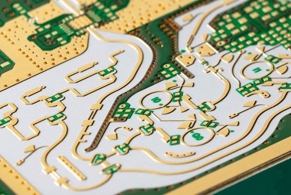
PCB impedance control
Different signal types require different impedance structures in PCB impedance control design.
Microstrip
A microstrip trace is routed on the outer layer of the PCB with a reference plane below.
Characteristics:
- Easier to manufacture
- Lower cost in pcba manufacturing
- More exposed to noise
Stripline
A stripline trace is embedded between two reference planes.
Characteristics:
- Better shielding
- More stable impedance
- Higher cost and complexity in PCB assembly
Differential Pairs
Differential impedance is used for high-speed signals.
Common examples:
- USB
- Ethernet
- LVDS
Maintaining consistent spacing between traces is critical for PCB impedance control in differential pairs.
Key Factors Affecting PCB Impedance Control
Trace Width and Thickness
Wider traces reduce impedance, while narrower traces increase it.
Designers must carefully calculate trace dimensions to meet impedance targets in pcba manufacturing.
Dielectric Material
The dielectric constant (Dk) of PCB material affects impedance.
- Higher Dk → lower impedance
- Lower Dk → higher impedance
Material consistency is critical for reliable pcb assembly results.
Distance to Reference Plane
The closer a trace is to the ground plane, the lower the impedance.
Controlling layer spacing is essential in PCB impedance control.
PCB Stack-Up Design
Stack-up defines layer arrangement and spacing.
A well-planned stack-up ensures consistent impedance across the board and improves manufacturability in pcba service.
Common Impedance Values
Typical impedance targets in PCB impedance control include:
- 50Ω (single-ended signals)
- 75Ω (video signals)
- 90Ω differential (USB)
- 100Ω differential (Ethernet, LVDS)
Meeting these targets is essential for high-performance smt pcb assembly products.
How to Design for PCB Impedance Control
impedance control PCB design
Define Requirements Early
Impedance requirements should be defined at the beginning of the design process in pcba manufacturing.
Work with Your Manufacturer
Different manufacturers have different capabilities.
Collaborating with your pcba service provider ensures your design matches real production conditions.
Use Impedance Calculators and Simulation
Design tools help predict impedance values based on stack-up and geometry.
Accurate simulation reduces trial-and-error in PCB assembly.
Maintain Consistent Routing
Avoid sudden changes in trace width or spacing.
Consistency is key to stable PCB impedance control.
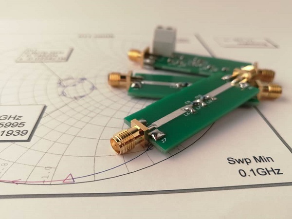
Impedance Testing and Verification
After fabrication, impedance must be verified.
Common methods:
- TDR (Time Domain Reflectometry)
- Impedance test coupons
Testing ensures the actual PCB meets design specifications in pcba manufacturing.
Impact on SMT PCB Assembly
While impedance is mainly a design and fabrication concern, it also affects smt pcb assembly.
- Proper impedance design reduces rework caused by signal issues
- Improves overall product reliability
- Reduces debugging time
A well-controlled impedance design ensures smoother production in pcba service.
Common Mistakes in PCB Impedance Control
controlled impedance PCB
Avoid these common errors:
- Ignoring stack-up during design
- Not consulting the manufacturer
- Inconsistent trace routing
- Incorrect differential pair spacing
- Using wrong material parameters
These mistakes can lead to signal failures and increased costs in pcba manufacturing.
Best Practices for Reliable Impedance Control
To achieve stable PCB impedance control, follow these best practices:
- Define impedance requirements clearly
- Use standard materials whenever possible
- Keep routing consistent
- Collaborate with your pcba service provider
- Verify impedance with testing
These steps ensure reliable performance in high-speed PCB assembly.
Conclusion
PCB impedance control is a fundamental aspect of modern PCB design, especially for high-speed and high-frequency applications. By understanding key factors such as trace geometry, materials, and stack-up, you can ensure stable signal performance.
In today’s advanced electronics industry, proper impedance control not only improves product quality but also supports efficient smt pcb assembly and scalable pcba manufacturing. Working closely with a professional pcba service provider ensures your design performs as expected from prototype to mass production.