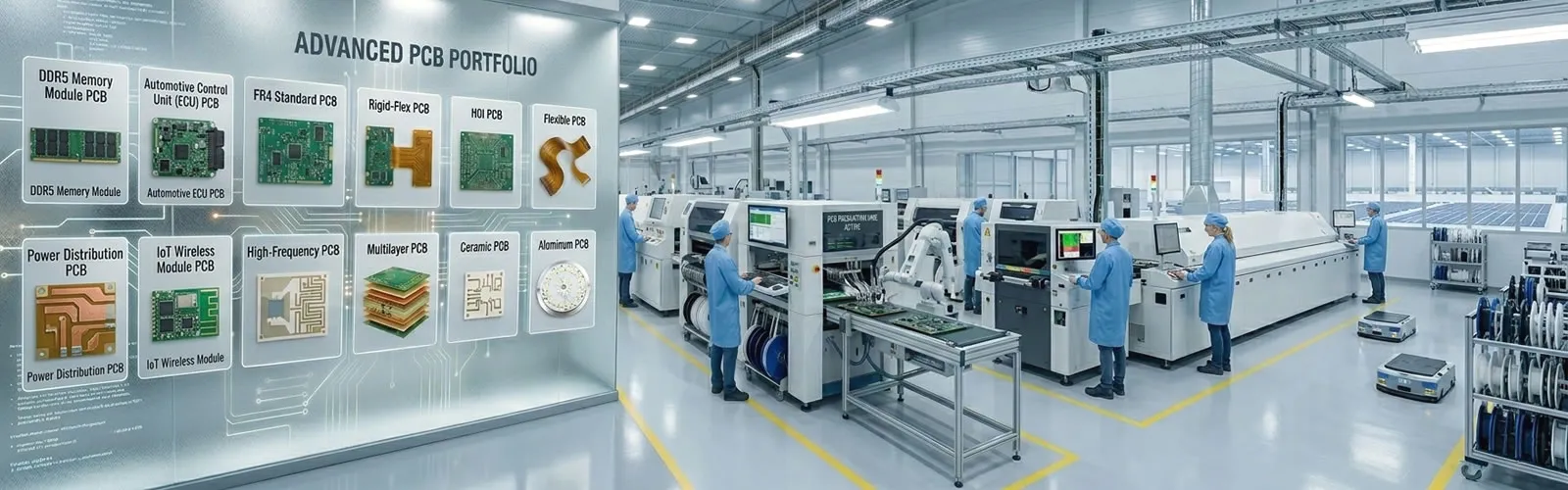
PCB Manufacturing – Prototype to Mass Production
One-Stop Solutions for Rigid, Flexible, Rigid-Flex, HDI, and High-Speed PCBs
As a ISO9001:2015 and UL 94V-0 certified PCB manufacturer, we provide end-to-end PCB manufacturing services – from prototype validation to high-volume production. Unlike fab-only shops that focus solely on fabrication, we offer complete solutions including PCB fabrication, assembly, testing, and box build.
Whether you need standard FR4 boards, high-density HDI, flexible circuits, or ceramic substrates, we deliver consistent quality, competitive pricing, and reliable lead times – all under one roof.
One supplier. One quality standard. One point of contact. From prototype to production.
Our PCB Fabrication Services


Our PCB Manufacturing Capabilities
| Parameter | Our Capability |
|---|---|
| Layer count | 1 to 12 layers (higher on request) |
| Board thickness | 0.4mm to 3.2mm |
| Copper weight | 0.5 oz to 6 oz |
| Min trace width/spacing | 3 mil / 3 mil (0.075mm) – HDI: 2 mil available |
| Min drill size | 0.15mm mechanical, 0.10mm laser microvia |
| Surface finishes | ENIG, HASL Lead-Free, OSP, Immersion Silver, Immersion Tin, Hard Gold |
| Solder mask colors | Green, Blue, Red, Black, White, Yellow, Purple, Matt colors |
| Special capabilities | Controlled impedance, heavy copper, blind/buried vias, via-in-pad |
Product Categories
We manufacture a full range of PCB types to meet diverse application requirements.
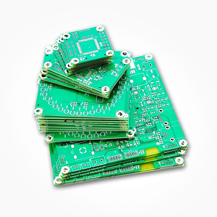
FR4 PCB – Standard Multilayer Circuit Boards
The workhorse of electronics. FR4 PCBs offer proven reliability at the lowest cost.
| Feature | Detail |
|---|---|
| Layer count | 1 to 12 layers |
| Material | FR4 (Standard TG or High TG 170°C) |
| Thickness | 0.6mm to 2.4mm |
| Applications | Industrial controls, consumer electronics, power supplies, IoT devices |
Typical customer: Engineers and procurement managers seeking reliable, cost-effective standard boards for volume production.
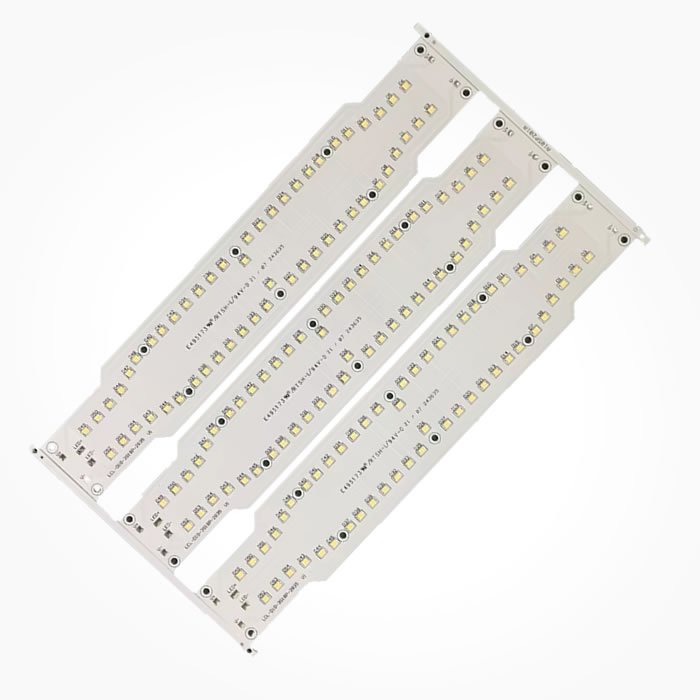
LED PCB – Aluminum Clad for High Power Lighting
Aluminum-backed PCBs designed for superior heat dissipation in LED lighting applications.
| Feature | Detail |
|---|---|
| Base material | Aluminum core (1.0mm to 3.2mm) |
| Copper weight | 1 oz to 4 oz |
| Thermal conductivity | 1W/mK to 3W/mK |
| Applications | LED lighting, automotive lighting, high-power modules |
Typical customer: Lighting manufacturers requiring thermal management for high-power LED arrays.
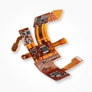
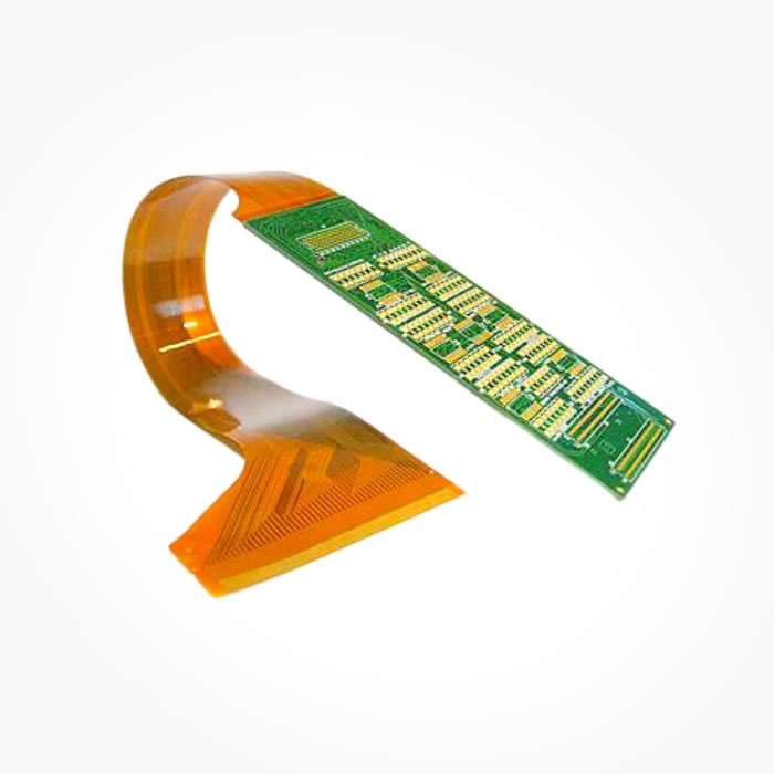
Flexible PCB / FPC – Bendable Circuits for Tight Spaces
Ultra-thin polyimide-based circuits that bend, fold, and twist – ideal for compact designs.
| Feature | Detail |
|---|---|
| Layer count | 1 to 6 layers (8 on request) |
| Thickness | 0.1mm to 0.4mm |
| Copper type | RA copper (rolled annealed) – standard |
| Bend radius | Static: 10x thickness / Dynamic: 30x thickness |
| Applications | Wearables, medical devices, cameras, foldable phones |
Typical customer: Design engineers needing thin, lightweight circuits for space-constrained products.
Rigid Flex PCB – Rigid + Flexible in One Board
Combines rigid FR4 sections (for heavy components) with flexible polyimide sections (for bending). Replaces rigid PCB + cable + connector assemblies.
| Feature | Detail |
|---|---|
| Rigid layers | 2 to 12 layers |
| Flex layers | 1 to 4 layers |
| Rigid sections | 2 to 8+ sections per board |
| Applications | Laptops, medical devices, aerospace, industrial robotics |
Typical customer: Engineers eliminating connectors and cables in high-reliability, space-constrained designs.
HDI PCB – High Density Interconnect for Miniaturization
Fine traces (3/3 mil), microvias (0.10mm laser), and higher layer counts for compact, high-performance devices.
| Feature | Detail |
|---|---|
| Min trace/spacing | 3 mil / 3 mil (2 mil available) |
| Microvia size | 0.10mm laser |
| Layer count | 4 to 12 layers |
| Via types | Blind, buried, stacked, staggered |
| Applications | Smartphones, tablets, medical implants, aerospace |
Typical customer: Advanced product developers pushing the limits of miniaturization.
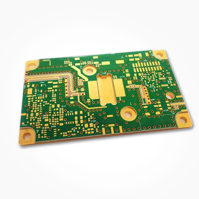
High Speed Digital PCB – Controlled Impedance for Signal Integrity
Precision-engineered PCBs for high-frequency digital signals – USB, Ethernet, HDMI, DDR, PCIe.
| Feature | Detail |
|---|---|
| Impedance control | 50Ω / 90Ω / 100Ω ±10% (±8% or ±5% available) |
| Material | High TG FR4 or low-loss materials |
| Testing | TDR (Time Domain Reflectometry) with test report |
| Applications | Servers, networking, telecom, high-speed ADCs |
Typical customer: Hardware engineers designing high-speed digital interfaces requiring signal integrity.
Ceramic Substrate PCB – Ultra-High Thermal Conductivity
Alumina (Al₂O₃) or Aluminum Nitride (AlN) based PCBs for extreme thermal and reliability requirements.
| Feature | Detail |
|---|---|
| Material | Alumina (96%/99.6%) or Aluminum Nitride |
| Thermal conductivity | 20W/mK to 180W/mK (AlN: 170-230W/mK) |
| CTE match | Close to silicon – ideal for direct die attachment |
| Applications | High-power LEDs, power modules, RF/microwave, aerospace |
Typical customer: Engineers requiring the highest thermal performance for power electronics.
Manufacturing & Quality Control Process
We follow a strict, documented manufacturing process to ensure consistent quality batch after batch.
| Step | Process | Quality Check |
|---|---|---|
| 1 | Material receiving | Incoming material inspection (IQC) – copper foil, prepreg, laminate |
| 2 | Inner layer imaging | AOI after etching – catches opens/shorts |
| 3 | Lamination | Temperature/pressure monitoring – prevents voids |
| 4 | Drilling | Automated drill – depth control for blind vias |
| 5 | Plating | Thickness measurement – ensures copper fill |
| 6 | Outer layer imaging | AOI – verifies trace integrity |
| 7 | Solder mask / Coverlay | Visual inspection – alignment, coverage |
| 8 | Surface finish | Thickness testing – ENIG, HASL, OSP |
| 9 | Electrical test | 100% flying probe or fixture test – every board |
| 10 | Final inspection | OQC – dimension, appearance, packaging |
| 11 | Shipping | Secure packaging with COC and test reports |
Industries We Serve
| Industry | Typical Products | Key Requirements |
|---|---|---|
| Automotive | ECUs, BMS, LED lighting, sensors | IATF 16949 processes, PPAP, wide temperature |
| Medical | Patient monitors, infusion pumps, endoscopes | High reliability, cleanliness, traceability |
| Industrial | PLCs, HMIs, motor drives, power supplies | 24/7 operation, noise immunity, long life |
| Consumer | Smart home, wearables, IoT devices | High volume, cost optimization |
| Telecom | Routers, switches, base stations | Controlled impedance, high layer count |
| Aerospace & Defense | Avionics, satellite electronics, radios | High reliability, MIL-spec, ITAR (on request) |
Ready to Start Your PCB Manufacturing Project?
👉Get a quick quote within 24 hours.
Upload your Gerber files and specifications. Our engineering team will review your design and provide a competitive quotation for prototype or production quantities.
✔ NDA Available ✔ Fast Quotation Within 24 Hours ✔ ISO Certified Factory ✔ One-stop PCB & PCBA Service
Frequently Asked Questions
What is your minimum order quantity (MOQ)?
No MOQ for prototypes. We accept orders as small as 5 pieces for design validation. For production, typical MOQ is 50-100 pieces for best pricing.
What certifications do you have?
ISO9001:2015 (quality management), UL 94V-0 (flammability rating), RoHS (lead-free), REACH compliance available upon request.
Do you offer PCB assembly (PCBA)?
Yes – turnkey PCB assembly available. Component sourcing + SMT + through-hole + functional testing + box build. One supplier, one invoice, one quality standard.
What is your typical lead time?
Prototypes (1-20 pcs): 3-7 days (rigid), 7-10 days (flex/rigid-flex). Production: 7-15 days depending on quantity and complexity. Express service available.
How do you protect my intellectual property?
NDA available. Secure file handling, access-controlled systems, confidential process. Your design files are never shared outside our engineering team. We never reuse your design for other customers.
Can you do controlled impedance?
Yes – 50Ω, 90Ω, 100Ω standard. Tighter tolerances (±8% or ±5%) available. TDR test reports included.
What file formats do you accept?
Gerber RS-274-X preferred. Also accept ODB++, IPC-2581, and PCB design files (Altium, Eagle, KiCad, PADS). Free DFM review included.
Do you offer free DFM review?
Yes – free DFM review for all orders. We check trace/spacing, annular ring, drill-to-copper, solder mask slivers, and stackup. Report provided within 24 hours.
What shipping options do you offer?
DHL Express (2-4 days) – best for prototypes and urgent orders. FedEx, UPS, air freight (5-10 days), sea freight (25-40 days) – best for volume production. We handle customs clearance.
How do I get started?
Simple process:
Upload your Gerber files and specifications
Receive free DFM review within 24 hours
Get competitive quotation
Approve and we start production
100% electrical test before shipping
Secure worldwide delivery
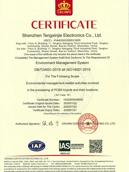
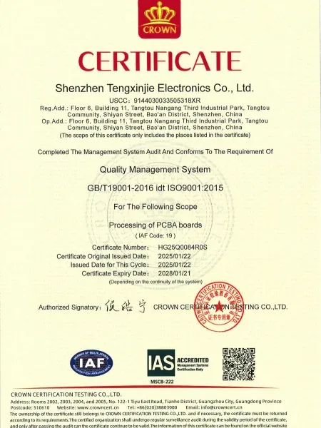
Our Certificates
Certificates
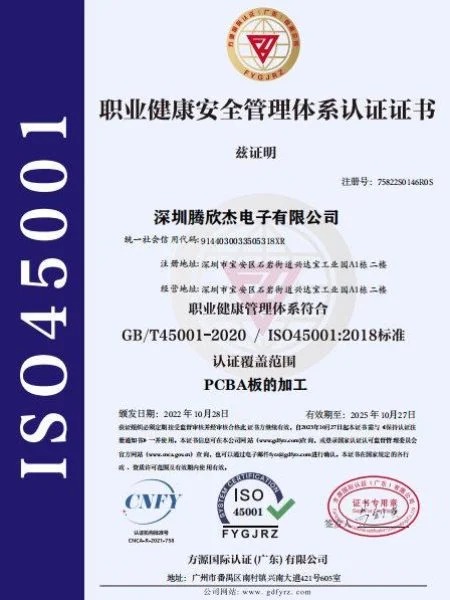
ISO 45001
- Phone:+1 (859) 254-6589
- Email:info@example.com
Certificates
- Phone:+1 (859) 254-6589
- Email:info@example.com
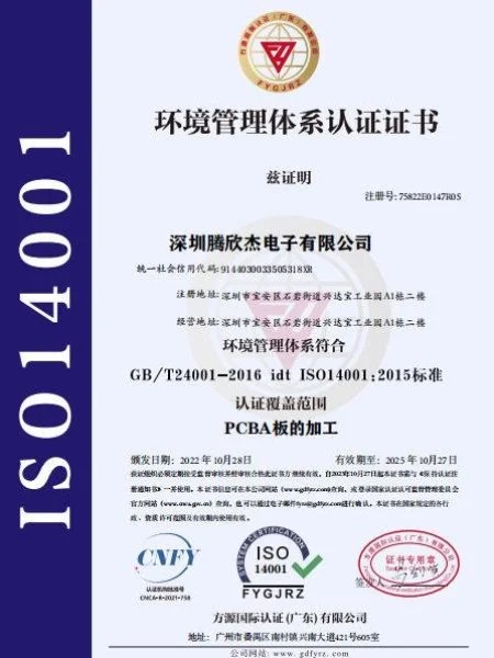
ISO 14001
- Phone:+1 (859) 254-6589
- Email:info@example.com
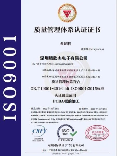
ISO 9001
- Phone:+1 (859) 254-6589
- Email:info@example.com
Certificates
- Phone:+1 (859) 254-6589
- Email:info@example.com
WeChat
Scan the QR Code with WeChat