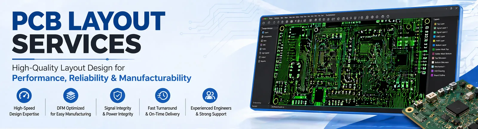
Professional PCB Layout Design for High-Performance Electronics
PCB layout is a critical stage in electronic product development, transforming circuit schematics into a manufacturable physical board. It involves precise component placement, signal routing, and optimization for performance, reliability, and manufacturability.
At Tengxinjie, we provide advanced PCB layout services tailored to meet the requirements of high-speed, high-density, and complex electronic systems.
PCB Layout Design Process
Our engineering workflow ensures accuracy and manufacturability, A well-executed layout directly impacts performance, EMI control, and reliability.
Our PCB Layout Capabilities
We support a wide range of PCB layout projects:
- High-speed digital PCB layout (DDR, PCIe, USB, HDMI)
- RF and microwave PCB layout
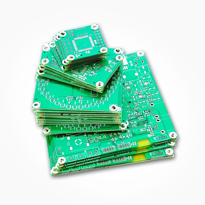
- Multilayer PCB layout (up to high layer count)
- HDI PCB layout (fine pitch, microvias)
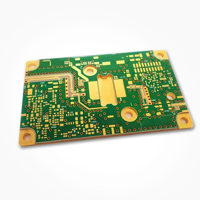
- Power electronics and high-current designs
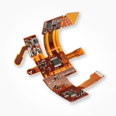
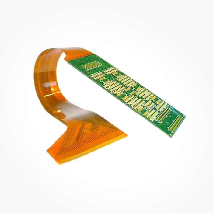
- Rigid, flexible, and rigid-flex PCB layout
Key Design Considerations
Our engineers follow industry best practices:
- Controlled impedance routing
- Signal integrity (SI) and power integrity (PI)
- EMI/EMC compliance
- Thermal management optimization
- High-density component placement
- Design for Manufacturability (DFM)
Quality Assurance System
We ensure every PCB layout meets strict engineering standards:
- Internal self-check procedures
- Peer design reviews
- Senior engineer validation
- DFM / DFT / SI / PI analysis
- Compliance with IPC standards (IPC-2221, IPC-7351)
Industries We Serve
Our PCB layout services are widely used in:
- Telecommunications (5G, networking equipment)
- Medical devices
- Industrial automation
- Consumer electronics
- Automotive electronics
- Aerospace and defense
Need professional PCB layout services for your project?
👉 We provide high-quality PCB design solutions including schematic design, multilayer layout, high-speed routing, and DFM optimization.
Send us your schematics or project requirements and receive a fast, accurate quotation from our experienced engineers.
✔ NDA Available ✔ Fast Quotation Within 24 Hours ✔ Professional Engineering Support
Frequently Asked Questions About PCB Layout
What is PCB Layout and why is it critical for my project?
PCB Layout is the physical arrangement of components, traces, vias, and copper planes on a printed circuit board. A well-optimized PCB Board Layout ensures signal integrity, proper power distribution, thermal management, and electromagnetic compatibility (EMC). Poor Circuit Board Layout can lead to crosstalk, voltage drops, EMI failures, and costly redesigns. At Tengxinjie, we deliver production-ready Pc Board Layout for your specific application.
What is the difference between PCB Layout, PCB Board Layout, and Circuit Board Layout?
PCB Layout, PCB Board Layout, and Circuit Board Layout are used interchangeably. All refer to the same essential process: component placement, trace routing, layer stackup design, and via placement on a printed circuit board. Pc Board Layout is simply a common abbreviation. Our focus is always on delivering a manufacturable, electrically robust layout regardless of the terminology.
What do your PCB Layout services include exactly?
Our PCB Layout services cover the full physical design scope: component placement optimization, routing (including high-speed, differential pairs, controlled impedance, and power traces), via placement, layer stackup design, design rule checking (DRC), and generation of all manufacturing outputs (Gerber, drill files, assembly drawings, pick-and-place files). We also provide PCB Layout Design for rigid, flex, and rigid-flex boards.
Do you offer PCB Layout Design as a standalone service?
Yes. PCB Layout Design is available as a standalone service. You provide a schematic or netlist, and we deliver a complete, manufacturable board layout. We work with industry-standard tools including Altium, Allegro, KiCad, and PADS. You are free to take the output PCB Board Layout files and have them fabricated and assembled by any manufacturer of your choice.
Can you handle complex Circuit Board Layout for high-speed or RF designs?
Absolutely. Our engineers are experienced in complex Circuit Board Layout designs including high-speed digital (DDR, PCIe, USB, HDMI), analog, mixed-signal, RF/microwave, and power electronics. We apply best practices for impedance control (±10%), crosstalk mitigation, grounding strategies, and decoupling capacitor placement. Your Pc Board Layout will be ready for signal integrity analysis and compliance testing.
What tools and file formats do you support for PCB Layout?
For PCB Layout, our designers use Altium Designer, Cadence Allegro, KiCad, and PADS. We accept schematics in native formats or PDF, and we deliver PCB Board Layout outputs as Gerber RS-274X, ODB++, IPC-2581, assembly drawings, pick-and-place files, and 3D STEP models. We ensure your Circuit Board Layout files are compatible with your fabrication and assembly requirements.
How do you ensure quality and manufacturability in your PCB Layout Design?
Quality is built into every PCB Layout Design through multiple checks: schematic vs. layout comparison (netlist verification), design rule checking (DRC) for spacing, width, and via rules, and a final DFM (Design for Manufacturing) review specifically for PCB Board Layout — covering annular rings, solder mask dams, silkscreen clarity, and panelization compatibility. We correct issues before you go to production.
How do I get started with your PCB Layout services?
To start, upload your schematic or netlist plus your PCB Layout requirements (layer count, board dimensions, impedance control needs, component placement constraints, etc.). Our team will review and provide a fixed-price quote for your Pc Board Layout project. We offer a free DFM check on the completed Circuit Board Layout before final file delivery.


WeChat
Scan the QR Code with WeChat