Professional PCBA Services for Smartphones
Introduction
PCB making machines are the foundation of modern electronics manufacturing, and nowhere is their importance more evident than in the smartphone industry. For B2B clients in Europe and North America, reliable PCBA services and PCB assembly services are critical to meeting the demands of a fast-paced market. Smartphones today require high-density interconnect boards, flexible PCBs, and advanced SMT processes to deliver performance, miniaturization, and durability.
Our company provides professional PCB assembly for smartphones, combining advanced equipment, engineering expertise, and strict quality control. By leveraging SMT assembly for smartphones, we help manufacturers accelerate time-to-market, reduce risks, and ensure compliance with international standards.
The Role of PCB Making Machines in Smartphone Manufacturing
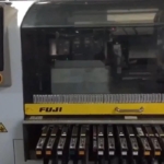
Smartphones integrate multiple technologies into compact designs. Without advanced pcb making machines, achieving precision and reliability would be impossible.
- Laser Drilling Systems: Create micro-vias essential for HDI boards.
- Etching Machines: Produce fine circuit patterns with minimal defects.
- Lamination Presses: Bond multiple layers to form complex multi-layer boards.
- SMT Pick-and-Place Machines: Place thousands of components per hour with micron-level accuracy.
- Reflow Ovens: Ensure strong and reliable solder joints.
- AOI and X-Ray Inspection Systems: Detect defects before products reach the market.
By integrating these machines into our production lines, we guarantee that every smartphone PCB meets the highest standards of performance and reliability.
Professional PCB Assembly for Smartphones
Our professional PCB assembly for smartphones supports critical functions:
- Processing Units: High-speed CPU and GPU integration requires precise soldering and signal integrity.
- Power Management: Efficient battery modules depend on reliable PCB layouts.
- Connectivity: RF circuits and antenna boards optimized for 5G and Wi-Fi.
- Display and Touch Modules: Flexible PCBs enable slim designs and foldable screens.
- Camera Systems: Multi-lens modules rely on compact, high-density PCBs.
These applications highlight why pcb making machines and SMT assembly for smartphones are indispensable in modern manufacturing.
Why B2B Clients Choose Us
European and North American B2B clients expect more than just manufacturing—they demand partnership, transparency, and scalability. Our services are designed to meet these expectations:
- End-to-End Solutions: From prototyping to mass production.
- Global Compliance: IPC, ISO, and RoHS certifications.
- Scalable Capacity: Flexible production lines to handle small or large orders.
- Engineering Support: Design-for-manufacturing (DFM) consultation to optimize layouts.
- Supply Chain Reliability: Secure sourcing of components with full traceability.
- Cost Efficiency: Competitive pricing without compromising quality.
Quality Assurance and Risk Management
Quality is non-negotiable in smartphone manufacturing. We implement strict quality control measures at every stage:
- Incoming Material Inspection: Ensuring all components meet specifications.
- In-Process Monitoring: Real-time data collection from pcb making machines.
- Final Testing: Functional tests, burn-in tests, and reliability checks.
- Traceability Systems: Every board is tracked from raw material to finished product.
For B2B clients, this means reduced risk, fewer recalls, and stronger market confidence.
Supply Chain and Risk Management
In addition to manufacturing, supply chain management plays a critical role in smartphone production. Component shortages and logistical challenges can delay product launches. We mitigate these risks by:
- Diversified Sourcing: Partnering with multiple suppliers to ensure availability.
- Inventory Management: Maintaining buffer stocks for critical components.
- Traceability Systems: Tracking every component from supplier to final assembly.
For B2B clients, this means reduced risk and greater confidence in meeting production schedules.
Engineering Support for B2B Clients
Beyond manufacturing, we provide engineering support to optimize PCB designs. Our services include:
- Design-for-Manufacturing (DFM) Analysis: Identifying potential issues before production.
- Thermal Management Solutions: Ensuring efficient heat dissipation in smartphones.
- Signal Integrity Testing: Guaranteeing high-speed data transmission.
- Prototype Development: Accelerating product validation and market entry.
This holistic approach ensures that our clients not only receive high-quality PCBs but also benefit from technical expertise that enhances their product designs.
Long-Term Partnership Approach
We understand that B2B clients seek more than just a supplier—they want a partner who can support their growth. Our partnership approach includes:
- Dedicated Account Managers: Providing personalized support.
- Regular Performance Reviews: Ensuring continuous improvement.
- Joint Development Projects: Collaborating on new technologies.
- After-Sales Support: Offering technical assistance even after delivery.
This long-term commitment strengthens relationships and helps clients achieve sustained success in the smartphone market.
Industry Trends and Future Outlook
The smartphone industry is evolving rapidly, with trends such as foldable displays, AI-driven applications, and 5G connectivity shaping the future. These innovations place even greater demands on pcb making machines and PCBA services.
- Miniaturization: Smaller devices require more complex PCB designs.
- High-Speed Connectivity: 5G and Wi-Fi 7 demand advanced RF PCB solutions.
- Sustainability: Eco-friendly materials and RoHS compliance are increasingly important.
- Customization: B2B clients seek tailored solutions to differentiate their products.
By staying ahead of these trends, we ensure that our clients remain competitive in the global market.
PCB making machines are the driving force behind modern electronics manufacturing. In the smartphone industry, their role is indispensable. For B2B clients in Europe and North America, reliable PCBA services and PCB assembly services are critical to meeting the demands of a competitive market. Smartphones today require high-density interconnect boards, flexible PCBs, and advanced SMT processes to achieve performance, miniaturization, and durability.
Our company specializes in professional PCB assembly for smartphones, combining advanced equipment, engineering expertise, and strict quality control. By leveraging SMT assembly for smartphones, we help manufacturers accelerate time-to-market, reduce risks, and ensure compliance with international standards.
The Importance of PCB Making Machines
Smartphones integrate multiple technologies into compact designs. Without advanced pcb making machines, achieving precision and reliability would be impossible.
- Laser Drilling Systems: Create micro-vias essential for HDI boards.
- Etching Machines: Produce fine circuit patterns with minimal defects.
- Lamination Presses: Bond multiple layers to form complex multi-layer boards.
- SMT Pick-and-Place Machines: Place thousands of components per hour with micron-level accuracy.
- Reflow Ovens: Ensure strong and reliable solder joints.
- AOI and X-Ray Inspection Systems: Detect defects before products reach the market.
By integrating these machines into our production lines, we guarantee that every smartphone PCB meets the highest standards of performance and reliability.
Professional PCB Assembly for Smartphones
Our professional PCB assembly for smartphones supports critical functions:
- Processing Units: High-speed CPU and GPU integration requires precise soldering and signal integrity.
- Power Management: Efficient battery modules depend on reliable PCB layouts.
- Connectivity: RF circuits and antenna boards optimized for 5G and Wi-Fi.
- Display and Touch Modules: Flexible PCBs enable slim designs and foldable screens.
- Camera Systems: Multi-lens modules rely on compact, high-density PCBs.
These applications highlight why pcb making machines and SMT assembly for smartphones are indispensable in modern manufacturing.
Why B2B Clients Partner With Us
European and North American B2B clients expect more than just manufacturing—they demand partnership, transparency, and scalability. Our services are designed to meet these expectations:
- End-to-End Solutions: From prototyping to mass production.
- Global Compliance: IPC, ISO, and RoHS certifications.
- Scalable Capacity: Flexible production lines to handle small or large orders.
- Engineering Support: Design-for-manufacturing (DFM) consultation to optimize layouts.
- Supply Chain Reliability: Secure sourcing of components with full traceability.
- Cost Efficiency: Competitive pricing without compromising quality.
Quality Assurance and Risk Management
Quality is non-negotiable in smartphone manufacturing. We implement strict quality control measures at every stage:
- Incoming Material Inspection: Ensuring all components meet specifications.
- In-Process Monitoring: Real-time data collection from pcb making machines.
- Final Testing: Functional tests, burn-in tests, and reliability checks.
- Traceability Systems: Every board is tracked from raw material to finished product.
For B2B clients, this means reduced risk, fewer recalls, and stronger market confidence.
Engineering Support for B2B Clients
Beyond manufacturing, we provide engineering support to optimize PCB designs. Our services include:
- Design-for-Manufacturing (DFM) Analysis: Identifying potential issues before production.
- Thermal Management Solutions: Ensuring efficient heat dissipation in smartphones.
- Signal Integrity Testing: Guaranteeing high-speed data transmission.
- Prototype Development: Accelerating product validation and market entry.
This holistic approach ensures that our clients not only receive high-quality PCBs but also benefit from technical expertise that enhances their product designs.
Long-Term Partnership Approach
We understand that B2B clients seek more than just a supplier—they want a partner who can support their growth. Our partnership approach includes:
- Dedicated Account Managers: Providing personalized support.
- Regular Performance Reviews: Ensuring continuous improvement.
- Joint Development Projects: Collaborating on new technologies.
- After-Sales Support: Offering technical assistance even after delivery.
This long-term commitment strengthens relationships and helps clients achieve sustained success in the smartphone market.
Industry Trends and Future Outlook
The smartphone industry is evolving rapidly, with trends such as foldable displays, AI-driven applications, and 5G connectivity shaping the future. These innovations place even greater demands on pcb making machines and PCBA services.
- Miniaturization: Smaller devices require more complex PCB designs.
- High-Speed Connectivity: 5G and Wi-Fi 7 demand advanced RF PCB solutions.
- Sustainability: Eco-friendly materials and RoHS compliance are increasingly important.
- Customization: B2B clients seek tailored solutions to differentiate their products.
By staying ahead of these trends, we ensure that our clients remain competitive in the global market.
Conclusion
Smartphone manufacturing is a complex process that requires precision, reliability, and innovation. With advanced pcb making machines, comprehensive PCBA services and PCB assembly services, and a commitment to quality, we empower B2B clients in Europe and North America to stay competitive in the global market.
By choosing us as your partner, you gain access to cutting-edge technology, robust quality systems, and a dedicated team that understands the unique challenges of smartphone production. Together, we can build the future of mobile technology.