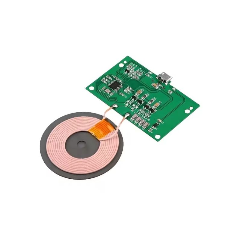

Wireless Charger PCBA Manufacturing for Stable and Efficient Power Transfer
We provide professional manufacturing solutions for wireless charger pcba projects designed for efficient inductive power transfer, thermal stability, and long-term operational reliability. Wireless charging systems are widely applied in smartphones, wearable devices, consumer electronics, automotive interiors, and IoT hardware where cable-free charging improves user convenience and product value.
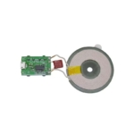
Compared with traditional wired power modules, wireless charging circuits require stricter layout precision and electromagnetic control. Coil alignment, signal stability, and heat management directly affect charging efficiency and product safety. Our manufacturing approach focuses on stable process control and consistent electrical performance across production batches.
Engineering Review for Wireless Charging Boards
Each wireless charger pcb assembly begins with a detailed engineering evaluation before mass production. This review analyzes copper thickness, trace width, coil interface layout, impedance matching, and thermal distribution across the board.
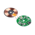
Proper layout and component positioning are critical in wireless power systems. The relationship between the transmitting coil, driver IC, and power management circuit must be optimized to reduce energy loss and electromagnetic interference. Our engineering team verifies manufacturability and assembly feasibility to ensure stable output performance under different load conditions.
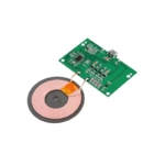
We support single-layer and multi-layer PCB structures depending on power level, charging protocol, and product design constraints.
Precision SMT Process for High-Frequency Circuits
Wireless charging modules operate at relatively high switching frequencies, which makes assembly precision essential. Our controlled smt pcb assembly process ensures accurate placement of controller ICs, MOSFETs, rectifiers, and passive components involved in power regulation and signal communication.
For each wireless charger smt pcb board, reflow temperature profiles are optimized to protect sensitive chips while maintaining strong solder integrity. Automated inspection systems verify solder joint quality and component alignment to reduce hidden defects.
Boards requiring additional shielding or structural reinforcement can be integrated with selective through-hole processes to enhance durability and mechanical strength.
Structured PCB Assembly Workflow
During full pcb assembly, we apply standardized quality control procedures to maintain consistent product performance. Wireless charging circuits require careful attention to signal routing and solder reliability, as minor deviations may affect charging efficiency or cause temperature rise.
Our workflow includes:
Incoming material verification
Solder paste inspection
Automated optical inspection
In-process monitoring
Visual and electrical verification
Each wireless charger pcba is inspected before shipment to ensure electrical continuity and structural integrity.
Integrated PCBA Service for OEM and ODM Projects
As a comprehensive pcba service provider, we support customers from prototype validation to volume production. Our service scope includes PCB fabrication coordination, component sourcing, SMT production, mixed-technology assembly, and manufacturing documentation support.
By integrating supply chain management and manufacturing control, we help customers reduce production risks and shorten product development cycles. This is particularly important for wireless charging devices entering competitive consumer markets where time-to-market and stability are critical.
Our scalable production model ensures consistent output capacity while maintaining stable quality standards.
Thermal Control and Long-Term Reliability
Wireless charging systems generate heat during power transmission. Without proper thermal management, charging efficiency may decrease and component lifespan may be reduced.
During manufacturing, we pay close attention to thermal pad soldering quality, copper plane balance, and component spacing to improve heat dissipation. Stable process control helps maintain consistent charging performance across different environmental conditions.
By combining controlled pcb assembly, precise smt pcb assembly, and systematic inspection procedures, we support reliable and durable wireless charger pcb assembly production for global customers.
Application Coverage
Our manufacturing solutions for wireless charger smt pcb board projects are suitable for:
Mobile phone charging pads
Smartwatch and wearable charging docks
Automotive wireless charging modules
Consumer electronic accessories
Embedded IoT charging platforms
Each project is produced with application-specific electrical and structural considerations to ensure performance stability and long-term operational reliability.
Reliable Manufacturing Partnership
Wireless power electronics demand both engineering understanding and disciplined production control. Through structured evaluation, stable pcb assembly, accurate smt pcb assembly, and integrated pcba service, we help customers bring dependable wireless charger pcba products to market with confidence.
If you are looking for a manufacturing partner capable of delivering consistent wireless charger pcb assembly solutions with scalable production capacity, our team is ready to support your project with professional and reliable execution.