PCBA Assembly & Electronics Manufacturing Services Provider

PCB Manufacturing Machine: 7 Powerful Benefits of Automatic Pick-and-Place Technology

Multilayer HDI PCB/High-Density Interconnect (HDI) PCB/


PCB&PCBA Manufacturer Pcb Machine for Multilayer Circuit Board Printing High Quality PCBA Product

Functional Application: Amplification

RAM: 8 GB

Model Number: PCBA

Place of Origin: Guangdong, China

Copper Thickness: 0.5 oz, 1 oz, 2 oz, 3 oz, 4 oz

Operating System: Android 11.0, Android 8.0, Android 6.0, Debian 10, Ubuntu 20.04, Android 7.1, Android 9.0

Product Name: PCB Board Assembly

Customization Support: Yes

Base Material: FR4, FR1-4

Board Thickness: 0.6 mm, 0.4 – 3.2 mm

Layer: 1 – 58 Layers

Certificate: ISO9001 / RoHS / CE

Surface Finishing: HASL Lead-Free

Solder Mask Color: Green, White

Personalized Requirements: Please contact us

Selling Units: Single item

Related products: High-Density Interconnect (HDI) PCB

  • Product Details
  • FAQS
  • Shipping & Delivery

Automatic PCB Pick-and-Place Machine: The Core PCB Manufacturing Machine for Modern Electronics Assembly

Introduction

In today’s global electronics industry, speed and precision are not optional — they are the foundation of competitiveness. For Western B2B clients outsourcing PCBA and PCB assembly services, the choice of equipment used by their manufacturing partner directly impacts product quality, delivery schedules, and compliance with international standards.

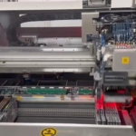
At the heart of modern assembly lines lies the Automatic PCB Pick-and-Place Machine, a specialized pcb manufacturing machine that ensures components are mounted with micron-level accuracy at industrial scale. This article explores the technical features, business benefits, and real-world applications of this machine, demonstrating why it is indispensable for B2B clients seeking reliable and scalable PCB assembly solutions.

Product Overview

The Automatic PCB Pick-and-Place Machine is designed to handle high-speed, high-precision component placement. It integrates robotic arms, advanced vision systems, and intelligent software to place thousands of components per hour with exceptional accuracy.

Key Specifications:

  • Placement Speed: Up to 70,000 components per hour
  • Accuracy: ±25 µm
  • Component Range: 0201, BGA, QFN, CSP, connectors
  • Board Size: 50 mm × 50 mm to 500 mm × 600 mm
  • Compliance: IPC-A-610 Class 2/3, ISO 9001, RoHS

Technical Features

1. Multi-Nozzle High-Speed Placement

  • Multiple nozzles operate simultaneously, dramatically increasing throughput.
  • Supports both miniature components and large connectors, ensuring flexibility.

2. Vision Alignment System

  • High-resolution cameras align each component with precision.
  • Eliminates offset errors, critical for fine-pitch ICs and high-density boards.

3. Flexible Feeding Options

  • Compatible with tape, tray, and tube packaging.
  • Quick feeder changeover supports both prototyping and mass production.

4. Intelligent Control Software

  • Stores placement profiles for different products.
  • Optimizes placement paths to reduce cycle time.

5. Inline Quality Control

  • Real-time defect detection for missing or misaligned components.
  • Generates detailed inspection reports, enhancing transparency for B2B clients.

Business Benefits for Western B2B Clients

Faster Time-to-Market

High-speed placement capabilities allow clients to accelerate product launches, reducing lead times and gaining a competitive edge.

Reduced Defect Rates

Vision alignment and inline inspection lower defect rates to below 1%, minimizing rework and warranty claims.

Cost Efficiency

Automation reduces labor costs and material waste, delivering long-term savings.

Compliance Assurance

Meeting IPC and ISO standards ensures smooth entry into regulated industries such as automotive, aerospace, and medical electronics.

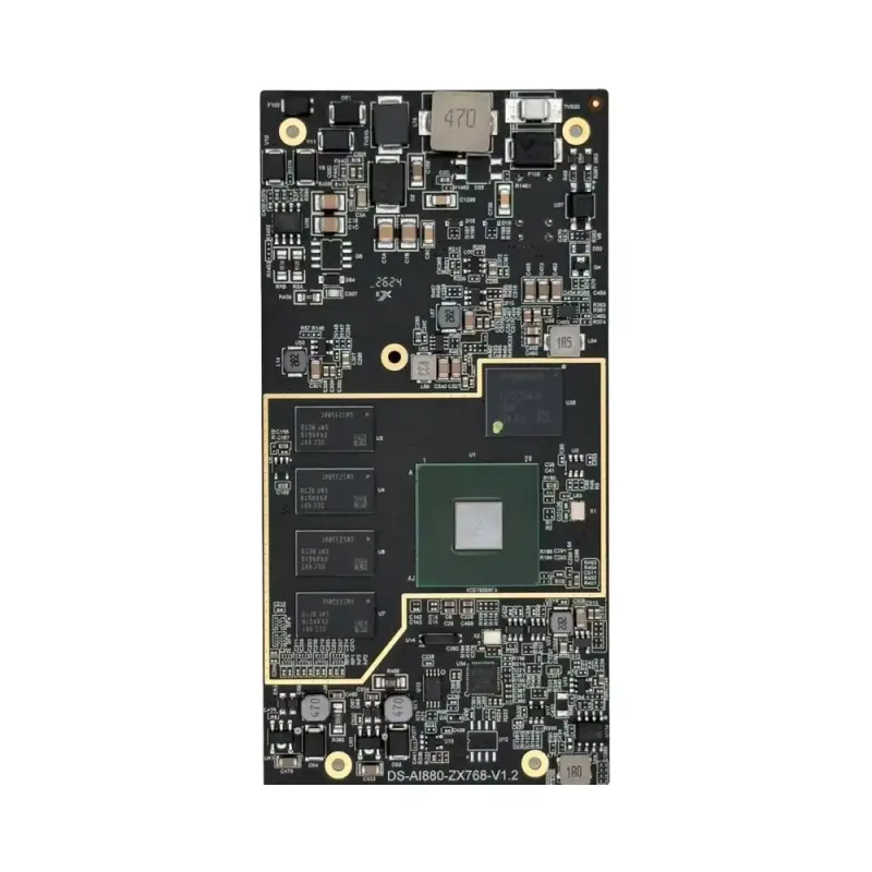
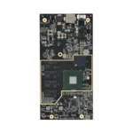
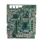
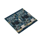
Case Study: Industrial IoT Gateway Boards

A Western client required Industrial IoT Gateway Boards with complex layouts and fine-pitch ICs.

  • Challenge: High component density and strict reliability requirements.
  • Solution: The Automatic PCB Pick-and-Place Machine ensured precise placement and minimized defects.
  • Result: Defect rate dropped below 0.9%, production lead time reduced by 30%, and compliance with international standards was guaranteed.

ROI Analysis

FactorTraditional PlacementAutomatic PCB Pick-and-Place MachineBusiness Impact
Accuracy±100 µm±25 µmImproved reliability
Defect Rate3–5%Lower warranty costs
Throughput500 boards/day2000 boards/dayFaster delivery
ComplianceLimitedIPC/ISO certifiedEasier market access

Alignment with Western B2B Expectations

  • Transparency: Machines generate detailed production logs and inspection reports.
  • Flexibility: Supports both prototype runs and mass production.
  • Sustainability: Lead-free soldering compatibility and energy-efficient operation.
  • Risk Management: Automated inspection reduces supply chain risks.

FAQ Section

Q1: Why is the Pick-and-Place Machine critical in PCB assembly? It determines the accuracy and speed of component placement, directly impacting product reliability.

Q2: How does this pcb manufacturing machine reduce costs? By lowering defect rates and minimizing manual labor, it reduces overall production costs.

Q3: Is it suitable for both prototypes and mass production? Yes, flexible feeders and quick changeover make it ideal for both scenarios.

Q4: Does it meet Western compliance standards? Absolutely. It complies with IPC-A-610, ISO 9001, and RoHS requirements.

Conclusion

The Automatic PCB Pick-and-Place Machine, a core pcb manufacturing machine, is the backbone of modern PCB assembly. By combining speed, precision, and compliance, it ensures that every component is placed correctly, contributing to the reliability of the final product.

For Western B2B clients, partnering with suppliers who invest in advanced pick-and-place technology is a guarantee of quality, scalability, and long-term business success. In a competitive global market, the right pcb manufacturing machine is not just equipment — it is a strategic asset.

Q: What is the standard ordering process for Tengxinjie’s PCBA manufacturing services?

A: PCB assembly steps:

  1. Submission of technical documents (Gerber files, BOM, pick-and-place, test requirements, etc.)
  2. Quotation review and lead-time confirmation
  3. Prototype build and customer approval (if required)
  4. Mass production with quality inspection (AOI, X-ray, functional testing)
  5. Final packaging and shipment
  6. After-sales technical support and feedback

This process ensures accuracy, traceability, and smooth transition from prototype to mass production.

Learn more: Tengxinjie Ordering Guide


Q: What Base Materials Does Tengxinjie Offer for PCB Manufacturing?

A: Tengxinjie offers a wide selection of PCB Base Materials, including standard FR4, HDI PCB, Flexible PCB, Rogers PCB, Teflon, copper-core, and aluminum substrates. With these options, you can easily select the most suitable material to ensure the best performance for your project.


Q: Does Tengxunjie accept small-batch or prototype orders?

A: Yes. We support small-batch production and prototype orders, typically with minimum order quantities ranging from 10 to 200 pieces.

However, small-batch production may result in higher unit costs, and certain electronic components have minimum order quantity (MOQ) requirements.
Partnering with a flexible PCBA supplier enables startups and R&D teams to advance product development without significant upfront investment.


Q: What is the typical PCBA lead time? What affects delivery time?

A: PCBA lead time depends on order size and project complexity. Typical estimates are:

  • Prototype builds: 5–10 working days

  • Small-batch production: 10–15 working days

  • Mass production: 15–30+ working days

Key factors that impact lead time include:

  • Component availability and specified brands

  • Turnkey service scope

  • PCB layer count and complexity

  • Testing and inspection requirements

An experienced PCBA manufacturer can help manage these factors to keep your project on schedule.


Q: How are PCBA boards packaged and shipped?

A: PCBA boards are packed according to their sensitivity and shipping method. Standard packaging includes:

  • ESD-safe anti-static bags

  • Bubble wrap, foam, or anti-static trays

  • Moisture-proof, labeled outer cartons with tracking information

For medical, automotive, or high-reliability electronics, cleanroom packaging or special handling is available.

Most PCBA suppliers support air freight, sea freight, and express courier based on order size and urgency.


Q: What are the advantages of turnkey PCBA and one-stop manufacturing?

A: Turnkey PCBA services mean the manufacturer handles everything — Electronic component sourcing, PCB fabrication, PCB assembly, testing, and logistics.

A reliable one-stop PCBA supplier helps customers:

  • Simplify supply chain management
  • Reduce sourcing and communication errors
  • Shorten production lead time
  • Speed up time-to-market

This is especially valuable for OEMs, startups, and engineering teams that need fast and stable production.


Q: How do we ensure the quality of electronic components used in assembly?

A: We maintain a rigorous supplier qualification process and a global procurement network, sourcing parts exclusively from authorized and trusted distributors. All incoming components undergo stringent inspection to verify authenticity and quality before being deployed.


Shipping Terms

Shipping costs are paid by the buyer.
We normally ship via DHL, UPS, FedEx, or TNT.
Alternatively, you may provide your own courier account or arrange delivery to your freight forwarder in China.

For large-volume orders, sea freight is available.


Delivery to Port (FOB Terms)

When shipping to a port, Tengxinjie is responsible for transporting the goods to the departure port.
All customs clearance, ocean freight, insurance, and onward transportation after that point are the responsibility of the buyer.

Tengxinjie can recommend reliable local freight forwarders upon request.
With the buyer’s authorization, Tengxinjie may also assist in coordinating shipping, with all related costs charged to the buyer.


Notice

The above shipping information is for reference only.
Tracking details and shipment updates will be provided once the order has been dispatched.

PCBA Shipping Delivery

PCBA Shipping Delivery

Prev:

Leave a Reply

Get a Quote ?

[contact-form-7 id="548" title="Contact Form"]