PCBA Assembly & Electronics Manufacturing Services Provider

B2B Small Wireless Charger PCBA Solutions - PCBA Manufacturer

Electric Mobility PCBA/Charging & Power PCBA/


Small Wireless Charger PCBA Solutions

Application: Charger Solutions

Layers: 1-32

Material: FR-4

Thickness: 0.2-4.5 mm

Copper: 1 oz

Surface Finish: HASL

Model: TXJ-EMCP-03

Use: Charger

Related products:   Electric Mobility PCBA

  • Product Details
  • FAQs
  • Shipping & Delivery

Small Wireless Charger PCBA for Compact and Efficient Charging Devices

As wireless charging technology continues to become more common in consumer electronics, manufacturers are increasingly focused on creating smaller, more efficient charging solutions. A well-designed small wireless charger pcba plays a critical role in enabling compact product designs while maintaining stable and efficient power transfer. Our manufacturing solutions are tailored for OEM manufacturers and electronics brands that require reliable circuit board production for modern wireless charging products.

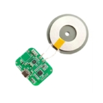
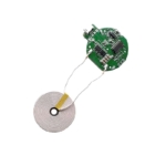
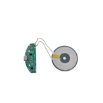
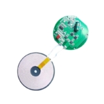
The small wireless charger pcba is designed to support compact wireless charging devices used in applications such as portable chargers, smart home accessories, wearable device chargers, desk charging stations, and other consumer electronics. These products require stable power management, precise circuit design, and high-quality manufacturing to ensure safe and efficient wireless energy transmission.

Our professional small wireless charger pcb assembly process ensures that every board is produced with precision and consistency. From component sourcing and PCB fabrication coordination to final assembly and inspection, each production stage is carefully managed to meet strict quality standards. This comprehensive manufacturing approach helps ensure that the final product performs reliably in real-world charging applications.

To achieve the high level of accuracy required for wireless charging circuits, we utilize advanced smt pcb assembly technology during production. Automated pick-and-place equipment allows precise mounting of electronic components on the small wireless charger smt pcb, even when working with compact layouts and fine-pitch components. Combined with automated solder paste printing and reflow soldering, this process ensures stable solder joints and consistent electrical performance across every production batch.

Our complete pcb assembly capability enables customers to move efficiently from prototype development to mass production. By integrating automated manufacturing systems with strict quality control procedures, we ensure that each small wireless charger pcba meets performance and reliability requirements. The combination of experienced engineers and modern manufacturing facilities allows us to deliver dependable production solutions for wireless charging electronics.

Quality assurance is particularly important for wireless charging devices, as stable circuit operation directly affects charging efficiency and device safety. For this reason, our small wireless charger pcb assembly workflow includes multiple inspection steps such as solder paste inspection, automated optical inspection (AOI), and functional testing. These procedures verify that each small wireless charger smt pcb operates according to design specifications before shipment.

In addition to manufacturing, we provide flexible pcba service options to meet the diverse needs of global B2B customers. Our pcba service can include design review, component sourcing support, prototype assembly, and large-scale production. By collaborating closely with customers during the early stages of product development, our engineering team helps optimize circuit designs for manufacturability and cost efficiency.

Another important advantage of our small wireless charger pcb assembly solution is scalability. Whether customers require small batches for product development or high-volume manufacturing for global distribution, our automated smt pcb assembly production lines are capable of supporting different order sizes while maintaining consistent quality and production efficiency.

Wireless charging products must balance compact size, efficient energy transfer, and long-term reliability. During the pcb assembly process, our engineering team pays close attention to circuit layout optimization, thermal management, and component stability to ensure reliable operation of each small wireless charger pcba.

With years of experience in pcb assembly, advanced smt pcb assembly technology, and comprehensive pcba service support, we provide reliable manufacturing solutions for wireless charging electronics. Our small wireless charger pcba production capability helps electronics manufacturers develop compact, efficient, and dependable wireless charging products for the global market.

Q: What is the standard ordering process for Tengxinjie’s PCBA manufacturing services?

A: PCB assembly steps:

  1. Submission of technical documents (Gerber files, BOM, pick-and-place, test requirements, etc.)
  2. Quotation review and lead-time confirmation
  3. Prototype build and customer approval (if required)
  4. Mass production with quality inspection (AOI, X-ray, functional testing)
  5. Final packaging and shipment
  6. After-sales technical support and feedback

This process ensures accuracy, traceability, and smooth transition from prototype to mass production.

Learn more: Tengxinjie Ordering Guide


Q: What Base Materials Does Tengxinjie Offer for PCB Manufacturing?

A: Tengxinjie offers a wide selection of PCB Base Materials, including standard FR4, HDI PCB, Flexible PCB, Rogers PCB, Teflon, copper-core, and aluminum substrates. With these options, you can easily select the most suitable material to ensure the best performance for your project.


Q: Does Tengxunjie accept small-batch or prototype orders?

A: Yes. We support small-batch production and prototype orders, typically with minimum order quantities ranging from 10 to 200 pieces.

However, small-batch production may result in higher unit costs, and certain electronic components have minimum order quantity (MOQ) requirements.
Partnering with a flexible PCBA supplier enables startups and R&D teams to advance product development without significant upfront investment.


Q: What is the typical PCBA lead time? What affects delivery time?

A: PCBA lead time depends on order size and project complexity. Typical estimates are:

  • Prototype builds: 5–10 working days

  • Small-batch production: 10–15 working days

  • Mass production: 15–30+ working days

Key factors that impact lead time include:

  • Component availability and specified brands

  • Turnkey service scope

  • PCB layer count and complexity

  • Testing and inspection requirements

An experienced PCBA manufacturer can help manage these factors to keep your project on schedule.


Q: How are PCBA boards packaged and shipped?

A: PCBA boards are packed according to their sensitivity and shipping method. Standard packaging includes:

  • ESD-safe anti-static bags

  • Bubble wrap, foam, or anti-static trays

  • Moisture-proof, labeled outer cartons with tracking information

For medical, automotive, or high-reliability electronics, cleanroom packaging or special handling is available.
Most PCBA suppliers support air freight, sea freight, and express courier based on order size and urgency.


Q: What are the advantages of turnkey PCBA and one-stop manufacturing?

A: Turnkey PCBA services mean the manufacturer handles everything — Electronic component sourcing, PCB fabrication, PCB assembly, testing, and logistics.

A reliable one-stop PCBA supplier helps customers:

  • Simplify supply chain management
  • Reduce sourcing and communication errors
  • Shorten production lead time
  • Speed up time-to-market

This is especially valuable for OEMs, startups, and engineering teams that need fast and stable production.


Q: How do we ensure the quality of electronic components used in assembly?

A: We maintain a rigorous supplier qualification process and a global procurement network, sourcing parts exclusively from authorized and trusted distributors. All incoming components undergo stringent inspection to verify authenticity and quality before being deployed.


Shipping Terms

Shipping costs are paid by the buyer.
We normally ship via DHL, UPS, FedEx, or TNT.
Alternatively, you may provide your own courier account or arrange delivery to your freight forwarder in China.

For large-volume orders, sea freight is available.


Delivery to Port (FOB Terms)

When shipping to a port, Tengxinjie is responsible for transporting the goods to the departure port.
All customs clearance, ocean freight, insurance, and onward transportation after that point are the responsibility of the buyer.

Tengxinjie can recommend reliable local freight forwarders upon request.
With the buyer’s authorization, Tengxinjie may also assist in coordinating shipping, with all related costs charged to the buyer.


Notice

The above shipping information is for reference only.
Tracking details and shipment updates will be provided once the order has been dispatched.

PCBA Shipping Delivery

PCBA Shipping Delivery

Prev:

Leave a Reply

Get a Quote ?

[contact-form-7 id="548" title="Contact Form"]