 PCB & PCBA Manufacturer

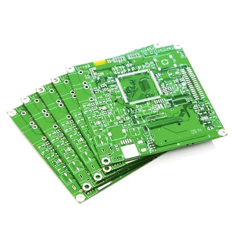
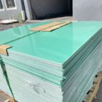
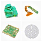
2 Layer FR4 PCB – Simple Design & Low Cost
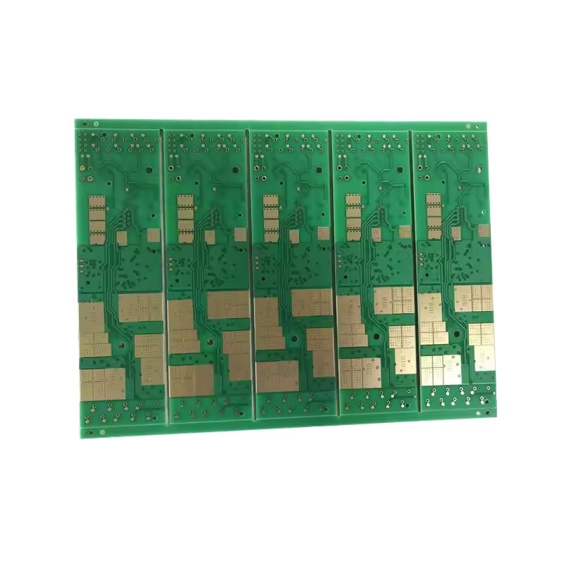
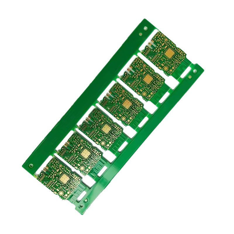
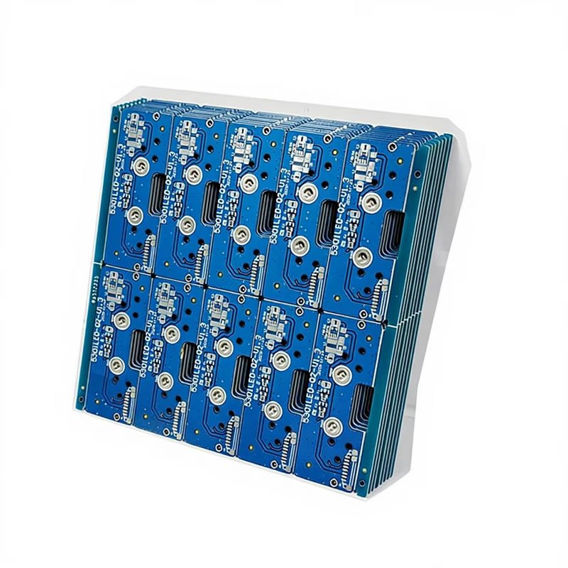
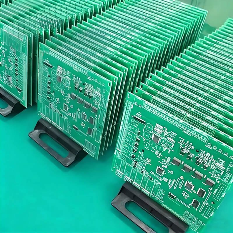
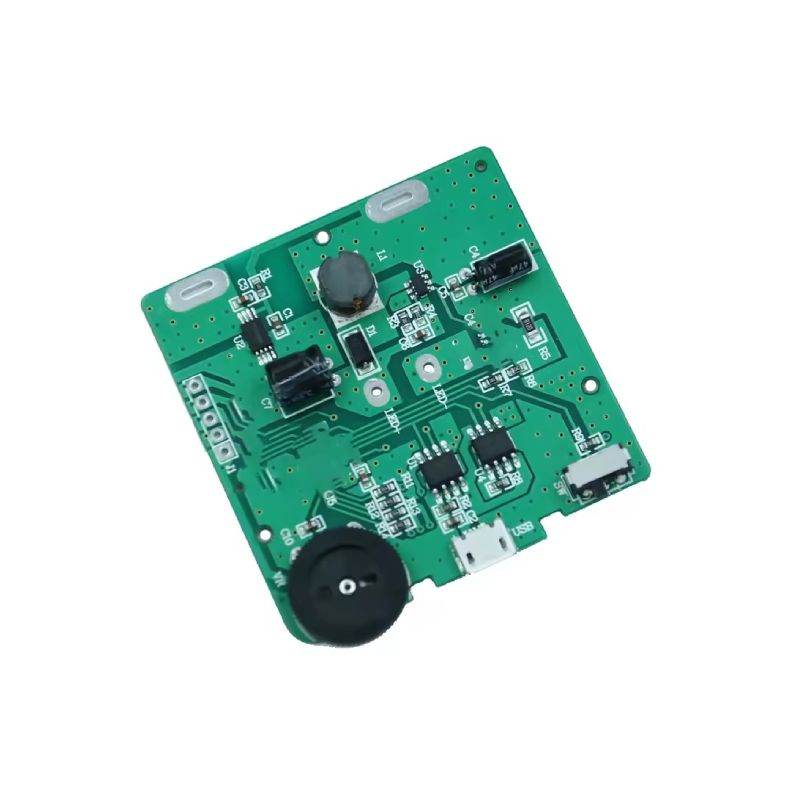
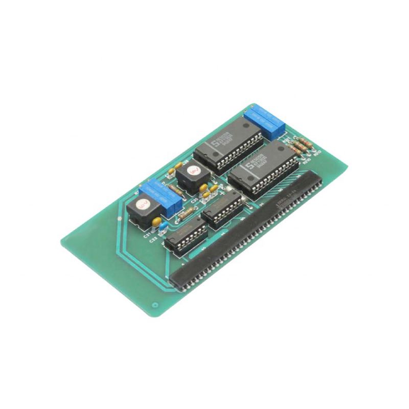
The 2 Layer FR4 PCB is the most basic and most affordable printed circuit board type. It consists of a top signal layer and a bottom signal layer, with no internal power or ground planes. For simple, low-speed, cost-sensitive applications – such as LED lighting modules, basic sensors, power supplies, and connector boards – the 2 layer FR4 PCB delivers reliable functionality at the lowest possible cost.
When to Choose a 2 Layer FR4 PCB
A 2 layer board is the right choice when your design meets these criteria:
| Criteria | Why 2 Layers Work |
|---|---|
| Low speed (under 10MHz) | Signal integrity issues are minimal |
| **No impedance control required | No controlled impedance needed – simpler design |
| Low component density | Plenty of space for routing on two layers |
| Cost is primary driver | 2 layers are 15-25% cheaper than 4 layers |
| Through-hole components dominate | Easy routing with wide traces |
If your design requires high-speed signals, tight impedance control, or dense BGA packages, a 4 layer or 6 layer board would be more suitable.
Typical Construction of 2 Layer FR4 PCB
| Layer | Function | Purpose |
|---|---|---|
| Layer 1 | Top Signal | Component placement & routing |
| FR4 Substrate | Dielectric material | Electrical isolation between layers |
| Layer 2 | Bottom Signal | Secondary routing & components |
Note: Unlike multilayer boards, there are no internal power or ground planes. Power and ground are distributed using copper pours or traces on the top and/or bottom layers.
Technical Specifications
| Parameter | Capability |
|---|---|
| Layer count | 2 layers (4, 6, 8, 10, 12 layers also available) |
| Base material | FR4 (TG 130°C – 170°C) |
| Board thickness | 0.6mm – 2.4mm (customizable) |
| Copper weight | 1 oz – 3 oz (standard 1 oz recommended) |
| Min trace width/spacing | 6 mil / 6 mil (0.15mm) – 4 mil available |
| Min annular ring | 5 mil |
| Min mechanical drill | 0.25mm |
| Surface finish | HASL Lead-Free, ENIG, OSP, Immersion Silver |
| Solder mask color | Green, Blue, Red, Black, White, Yellow |
| Silkscreen color | White, Black, Yellow |
Applications for 2 Layer FR4 PCB
| Application | Why 2 Layers? |
|---|---|
| LED lighting modules | Simple power delivery, low cost for high volume |
| Basic sensor boards | Temperature, humidity, motion – no high-speed needs |
| Power supply boards | AC-DC converters, simple regulators |
| Connector breakout boards | Routing signals between connectors – no complexity |
| Hobbyist & maker projects | Arduino shields, Raspberry Pi add-ons |
| Remote controls & keypads | Low component count, simple button matrix |
| Relay & switch boards | High current traces, simple routing |
2 Layer vs. 4 Layer FR4 PCB – Quick Comparison
| Feature | 2 Layer FR4 PCB | 4 Layer FR4 PCB |
|---|---|---|
| Layer count | 2 | 4 |
| Internal planes | None | Ground + Power |
| EMI performance | Basic – can radiate | Good – shielded by ground plane |
| Impedance control | Difficult, inconsistent | Practical and repeatable |
| Routing density | Low to medium | Medium to high |
| Cost | Lowest (baseline) | +15% to 25% |
| Turnaround time | Fastest (3-5 days) | 5-7 days |
| Best for | Simple, low-speed, cost-critical | Most commercial products |
Why Manufacture Your 2 Layer FR4 PCB With Us?
| Feature | What You Get |
|---|---|
| Quick turn prototype | 3-5 days for 2 layer prototypes |
| Mass production | 7-8 days for volume orders |
| AOI + Visual inspection | 100% electrical testing before shipment |
| UL & ISO9001 certified | Full traceability and quality system |
| Engineering support | DFM review before production – free of charge |
| Bulk pricing | Competitive rates for high-volume orders |
Order Process
Upload your Gerber files or design files
Receive engineering review and DFM report
Confirm order and proceed to fabrication
100% electrical test before packaging
Secure shipping with tracking