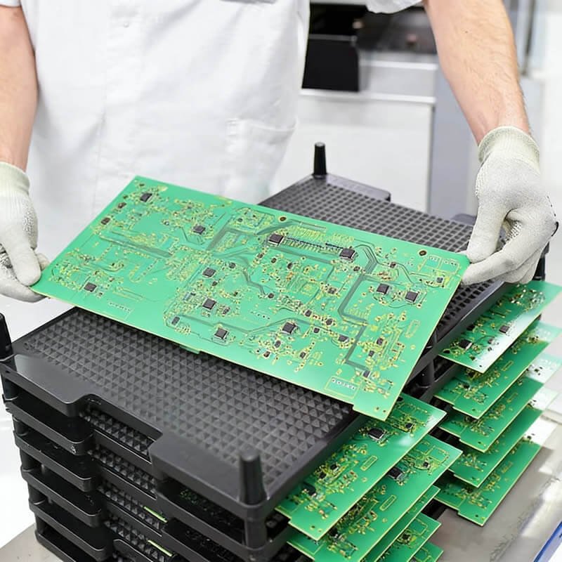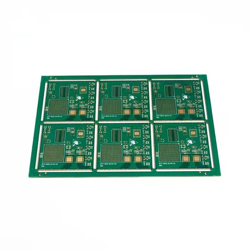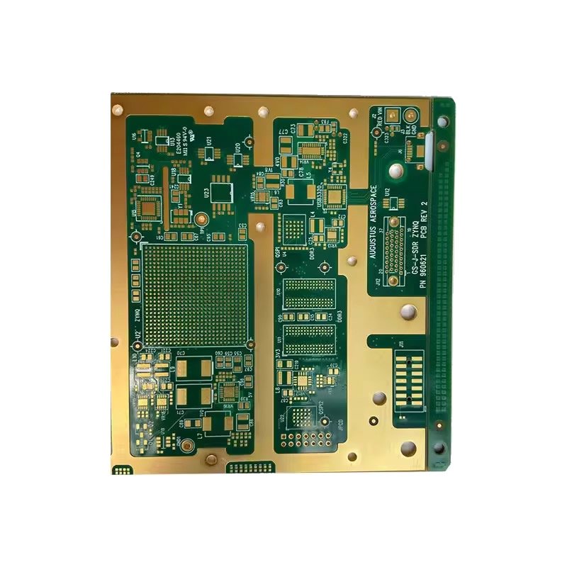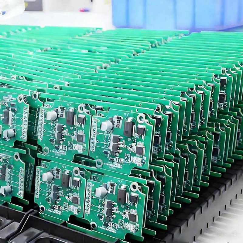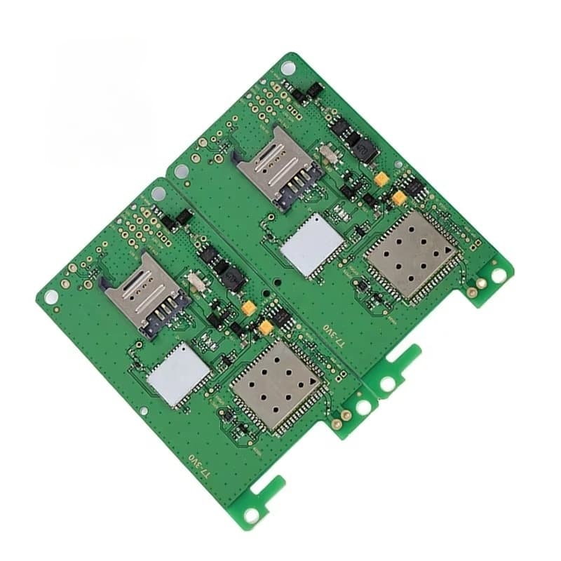
PCBA Assembly & Electronics Manufacturing Services Provider

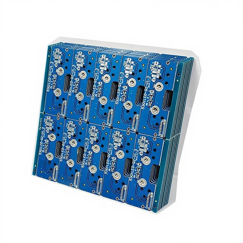
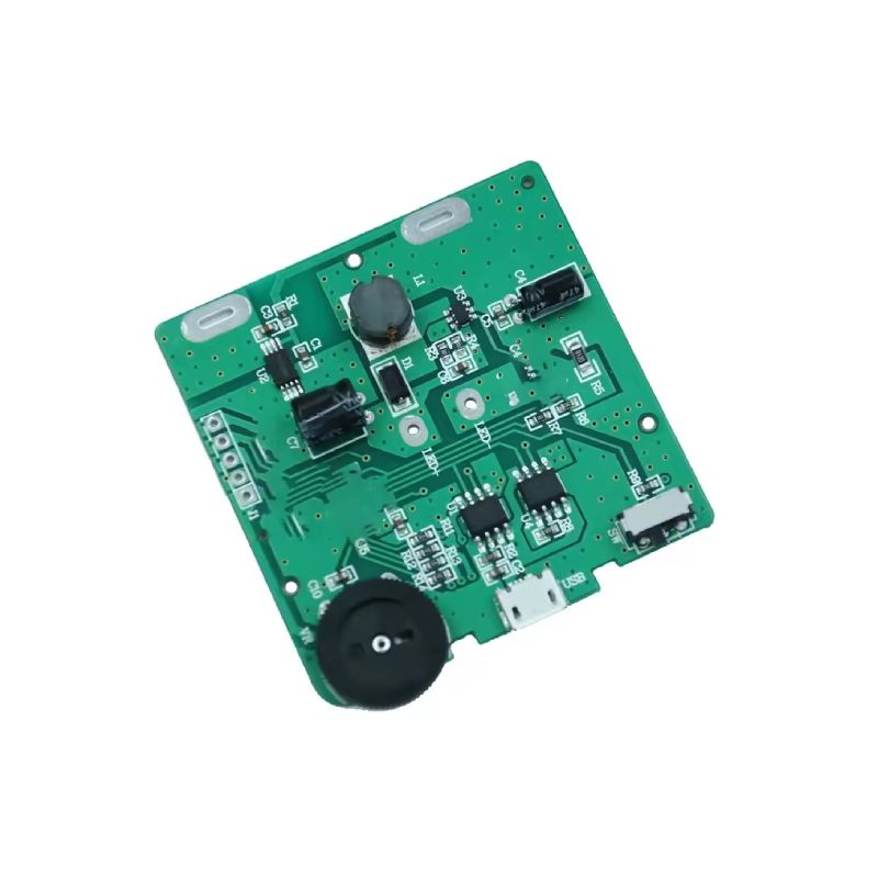
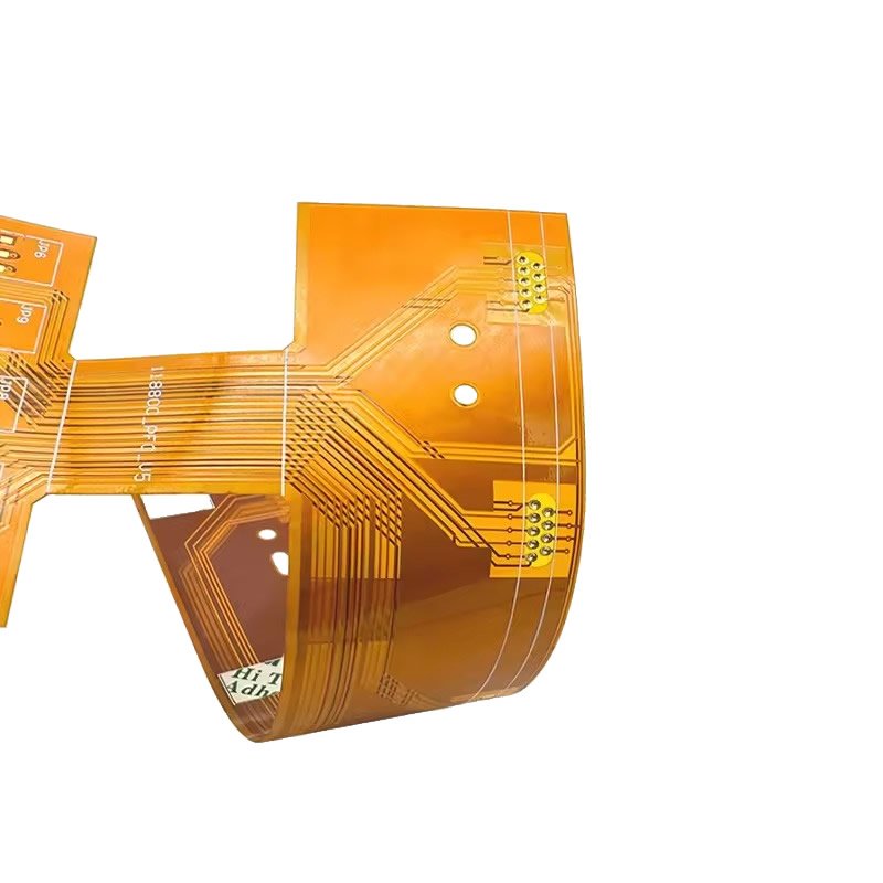
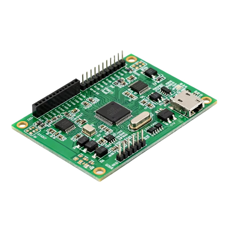
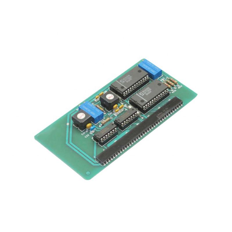
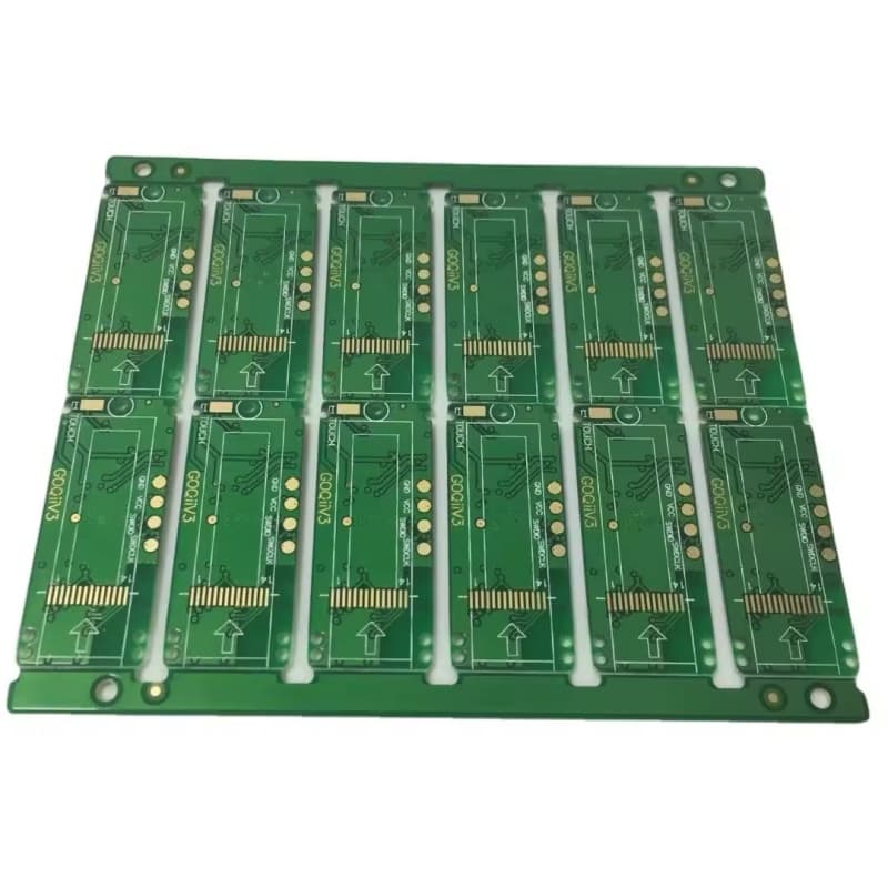
8 Layer FR4 PCB Manufacturer – High Density & Complex Routing

FR4 PCB/


8 Layer FR4 PCB – High Density & Complex Routing

  • 8 Layer FR4 PCB for high density & complex routing

  • Symmetrical stackup prevents board warpage

  • Two extra signal layers vs. 6-layer boards

  • Dedicated power & ground planes reduce noise

  • Improved EMI control for sensitive signals

  • Reduced crosstalk between adjacent layers

  • Controlled impedance: 50Ω / 90Ω / 100Ω

  • Min trace: 4 mil / 4 mil (3 mil available)

  • Quick turn: 5-7 days for prototypes

  • 100% electrical test – ISO9001 & UL certified

  • Product Details
  • FAQs
  • Shipping & Delivery

8 Layer FR4 PCB – Engineered for High Density & Complex Routing

As electronic devices become smaller, faster, and more feature-rich, the demand for higher layer count PCBs continues to grow. The 8 Layer FR4 PCB strikes an ideal balance between design complexity and manufacturing cost, making it a popular choice for applications that require dense component placement and sophisticated signal routing but do not yet require the extreme layer count of 10 or 12 layers.

Why Choose an 8 Layer FR4 PCB?

A standard 4 or 6 layer board may not provide enough routing channels for compact, high-performance designs. An 8 layer stackup offers:

  • Two additional internal signal layers – significantly more routing space without increasing board size

  • Improved power distribution – dedicated power and ground planes reduce voltage drop and noise

  • Better EMI control – strategic placement of ground planes shields sensitive signals

  • Reduced crosstalk – more distance and shielding between adjacent signal layers

Typical Layer Stackup for 8 Layer FR4 PCB

A common 8 layer stackup follows this structure:

LayerFunctionPurpose
Layer 1Top SignalComponent placement & routing
Layer 2GroundReference plane, shielding
Layer 3SignalHigh-speed or sensitive traces
Layer 4PowerCore voltage distribution
Layer 5GroundReturn path, isolation
Layer 6SignalSecondary routing
Layer 7GroundShielding for bottom layer
Layer 8Bottom SignalSecondary components & routing

This symmetrical stackup prevents board warpage and ensures manufacturing reliability.

Technical Specifications

ParameterCapability
Layer count8 layers (6 layers also available)
Base materialFR4 (TG 130°C – 170°C)
Board thickness1.0mm – 2.4mm (customizable)
Copper weight1 oz – 3 oz (inner & outer)
Min trace width/spacing4 mil / 4 mil (0.10mm)
Min annular ring4 mil
Min mechanical drill0.20mm
Surface finishHASL Lead-Free, ENIG, OSP, Immersion Silver
Solder mask colorGreen, Blue, Red, Black, White, Yellow
Silkscreen colorWhite, Black, Yellow

Applications for 8 Layer FR4 PCB

ApplicationWhy 8 Layers?
Industrial controllers (PLC, IPC)Mixed signal routing + reliable power distribution
Telecom infrastructureMultiple high-speed interfaces requiring isolation
Medical imaging devicesDense component placement in compact form factors
Automotive infotainmentCombines digital processing + audio + power in one board
Network switches & routersMany differential pairs + power integrity demands
Test & measurement equipmentPrecision analog + high-speed digital coexistence

Why Manufacture Your 8 Layer FR4 PCB With Us?

FeatureWhat You Get
Quick turn prototype5-7 days for 8 layer prototypes
Mass production12-15 days for volume orders
Impedance control±10% (tighter available on request)
AOI + Flying Probe100% electrical testing before shipment
UL & ISO9001 certifiedFull traceability and quality system
Engineering supportDFM review before production – free of charge

Order Process

  1. Upload your Gerber files and stackup

  2. Receive engineering review and DFM report

  3. Confirm order and proceed to fabrication

  4. 100% electrical test before packaging

  5. Secure shipping with tracking
Q1: When should I choose an 8 layer FR4 PCB over a 6 layer board?

A: Choose 8 layers when you have complex routing requirements and a 6 layer board forces you to use excessively long traces, create crowded routing channels, or compromise on power/ground plane distribution. 8 layers provide two additional internal routing layers, which significantly reduces layout difficulty for high-density designs.


Q2: What is the typical turnaround time for 8 layer FR4 PCB prototypes?

A: For prototype quantities (1-20 pieces) , typical lead time is 5-7 working days. For mass production (above 50 pieces) , lead time is approximately 12-15 working days, depending on layer stackup complexity and surface finish requirements.


Q3: Can you manufacture 8 layer FR4 PCB with controlled impedance?

A: Yes. We support controlled impedance requirements including 50Ω single-ended90Ω differential (USB), 100Ω differential (HDMI/Ethernet), and custom values. Our standard tolerance is ±10% . Tighter tolerance (±8% or ±5%) is available upon request for high-speed applications.


Q4: What surface finishes do you recommend for 8 layer FR4 PCB?

A:

  • ENIG (Electroless Nickel Immersion Gold) – Most recommended for complex 8 layer boards. Provides flat surface, good solderability, and long shelf life.

  • Lead-Free HASL – Cost-effective but less flat than ENIG. Suitable for standard SMT.

  • OSP – Lowest cost, but shorter shelf life. Good for high-volume, quick-turn assembly.

For high-density designs with fine-pitch components (under 0.5mm pitch), ENIG is strongly recommended.


Q5: What is the minimum trace width and spacing for your 8 layer FR4 PCB?

A: Our standard capability for 8 layer boards is 4 mil (0.10mm) trace width / 4 mil spacing. For advanced designs, we can support 3 mil / 3 mil with prior engineering review. Please contact us with your specific requirements.


Q6: Do you provide stackup recommendations?

A: Yes. If you do not have a defined stackup, our engineers will provide a customized 8 layer stackup recommendation based on your:

  • Total board thickness

  • Impedance requirements

  • Signal layer count needed

  • Manufacturing cost targets

This service is provided free of charge as part of our DFM review.

Shipping Terms

Shipping costs are paid by the buyer.
We normally ship via DHL, UPS, FedEx, or TNT.
Alternatively, you may provide your own courier account or arrange delivery to your freight forwarder in China.

For large-volume orders, sea freight is available.


Delivery to Port (FOB Terms)

When shipping to a port, Tengxinjie is responsible for transporting the goods to the departure port.
All customs clearance, ocean freight, insurance, and onward transportation after that point are the responsibility of the buyer.

Tengxinjie can recommend reliable local freight forwarders upon request.
With the buyer’s authorization, Tengxinjie may also assist in coordinating shipping, with all related costs charged to the buyer.


Notice

The above shipping information is for reference only.
Tracking details and shipment updates will be provided once the order has been dispatched.

PCBA Shipping Delivery

PCBA Shipping Delivery

Prev:

Leave a Reply

Get a Quote ?

[contact-form-7 id="548" title="Contact Form"]