 PCB & PCBA Manufacturer


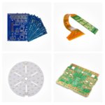
Power Supply FR4 PCB – Heavy Copper & High Current
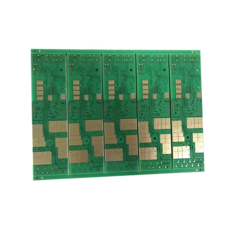
Power supplies – from AC-DC converters and DC-DC regulators to battery management systems and motor drives – demand PCBs capable of carrying high current without excessive heat generation or voltage drop. Standard 1 oz copper PCBs are insufficient for these applications. The Power Supply FR4 PCB is engineered with heavy copper weights (2 oz to 6 oz) and optimized thermal design to handle high current loads reliably.
Why Heavy Copper for Power Supply PCBs?
Standard PCBs use 1 oz copper (approximately 35µm thick), which can carry about 1-2 amps per 10 mil trace width depending on temperature rise. For high current applications, this requires extremely wide traces or multiple parallel traces, consuming valuable board space.
Heavy copper PCBs solve this problem:
| Copper Weight | Thickness | Current Capacity (per 10mm width, 10°C rise) | Best For |
|---|---|---|---|
| 1 oz (standard) | 35 µm | ~5A | Low power, signal |
| 2 oz | 70 µm | ~10A | Moderate power supplies |
| 3 oz | 105 µm | ~15A | Power converters |
| 4 oz | 140 µm | ~20A | Battery chargers, motor drives |
| 6 oz | 210 µm | ~30A | High power industrial supplies |
Key Design Features for Power Supply PCBs
| Feature | Purpose | How We Deliver |
|---|---|---|
| Heavy copper traces | Minimize resistance and IR drop | 2 oz to 6 oz copper on outer and/or inner layers |
| Wide power traces | Spread current evenly | No minimum width limit for power traces |
| Thermal vias | Conduct heat away from power components | Dense via arrays under MOSFETs and regulators |
| High TG material | Withstand heat from power dissipation | TG 170°C FR4 standard for power supplies |
| Thick board option | Support heavy components | Up to 2.4mm thickness for rigidity |
| Large pads & annular rings | Reliable soldering of power connectors | Oversized pads for TO-220, TO-247, screw terminals |
Technical Specifications for Power Supply FR4 PCB
| Parameter | Capability |
|---|---|
| Layer count | 2 to 12 layers (depending on complexity) |
| Base material | High TG FR4 (TG 170°C) – standard for power supplies |
| Copper weight | 2 oz to 6 oz (inner and outer layers) |
| Board thickness | 1.0mm – 2.4mm (thicker for heavy components) |
| Min trace width/spacing (signal) | 6 mil / 6 mil |
| Min trace width (power) | No minimum – as wide as needed |
| Min drill size | 0.25mm (power supply designs rarely need small vias) |
| Surface finish | HASL Lead-Free (preferred), ENIG, Immersion Silver |
| Solder mask | Green (standard), Blue, Red, Black, White |
| Additional features | Thermal vias, heat sink mounting holes, large copper pours |
Applications for Power Supply FR4 PCB
| Application | Copper Weight | Specific Requirements |
|---|---|---|
| AC-DC power supplies | 2-3 oz | High voltage isolation, large transformers |
| DC-DC converters | 2-4 oz | Multiple power planes, tight regulation |
| Battery management systems (BMS) | 3-6 oz | High charge/discharge currents, cell balancing |
| Motor drives & controllers | 4-6 oz | High inrush currents, PWM noise immunity |
| EV chargers | 4-6 oz | Very high current (20-50A), thermal management |
| Server power supplies | 3-4 oz | High density, efficiency, thermal vias |
| Industrial power inverters | 4-6 oz | Rugged design, wide temperature range |
| Solar inverters | 3-4 oz | Outdoor durability, high efficiency |
Standard vs. Heavy Copper – Quick Comparison
| Feature | Standard PCB (1 oz) | Heavy Copper PCB (3-6 oz) |
|---|---|---|
| Current capacity | Low (under 5A typical) | High (10-30A typical) |
| Trace width needed for 10A | ~200 mil (5mm) | ~60 mil (1.5mm) |
| Heat generation | Significant at high current | Lower due to less resistance |
| Board space efficiency | Poor for power | Excellent – narrower power traces |
| Cost | Baseline | +30% to 100% depending on copper weight |
| Manufacturing lead time | Standard | +2-3 days for heavy copper processing |
| Best for | Signal, low power | Power supplies, motor drives |
Thermal Management for Power Supply PCBs
Heat is the enemy of power supplies. Our Power Supply FR4 PCB incorporates multiple thermal management strategies:
| Thermal Feature | Benefit |
|---|---|
| Heavy copper | Lower resistance = less heat generation |
| Thermal vias | Conduct heat from top-layer components to bottom layer or heatsink |
| Copper pours | Large copper areas act as heat spreaders |
| High TG material | Maintains mechanical stability at high temperatures |
| Component placement optimization | Spacing heat-generating components to avoid hot spots |
Why Manufacture Your Power Supply FR4 PCB With Us?
| Feature | What You Get |
|---|---|
| Heavy copper capability | 2 oz to 6 oz – inner and outer layers |
| High TG standard | TG 170°C included at no extra charge for power supplies |
| Quick turn prototype | 7-10 days for heavy copper prototypes |
| Mass production | 12-15 days for volume orders |
| Thermal via support | Dense via arrays under power components |
| 100% electrical test | Including high current path verification |
| Engineering support | DFM review focused on power design challenges |
Order Process for Power Supply PCB
Upload your Gerber files – specify copper weight requirements
Receive DFM report with thermal recommendations
Confirm order – prototype or production quantity
Heavy copper fabrication – additional lamination cycles for thick copper
100% electrical test – including continuity on high current paths
Secure shipping with tracking