 PCB & PCBA Manufacturer
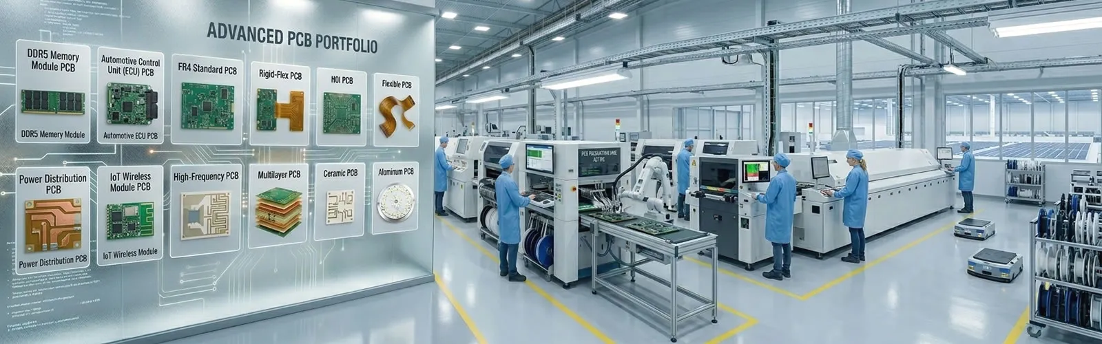
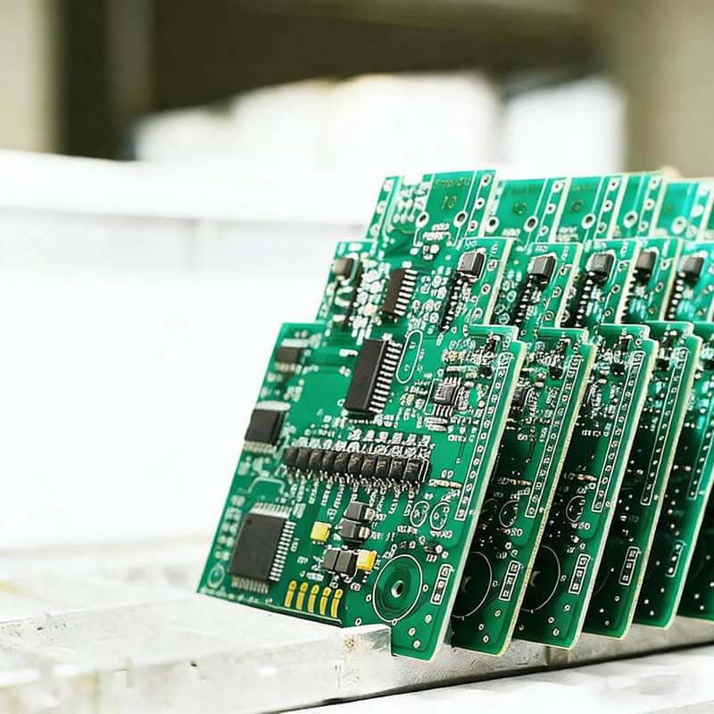
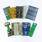
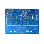
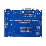
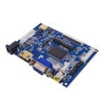
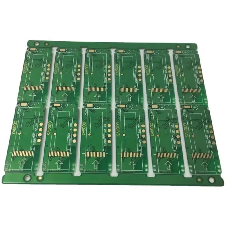
IoT Device FR4 PCB – Compact Design & Fast Turn
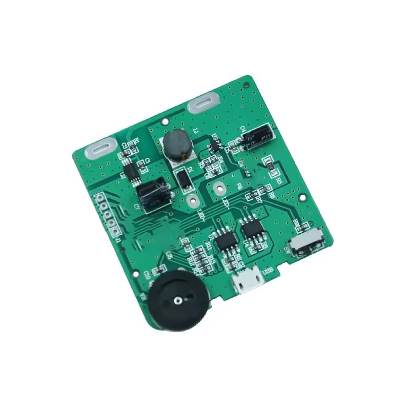
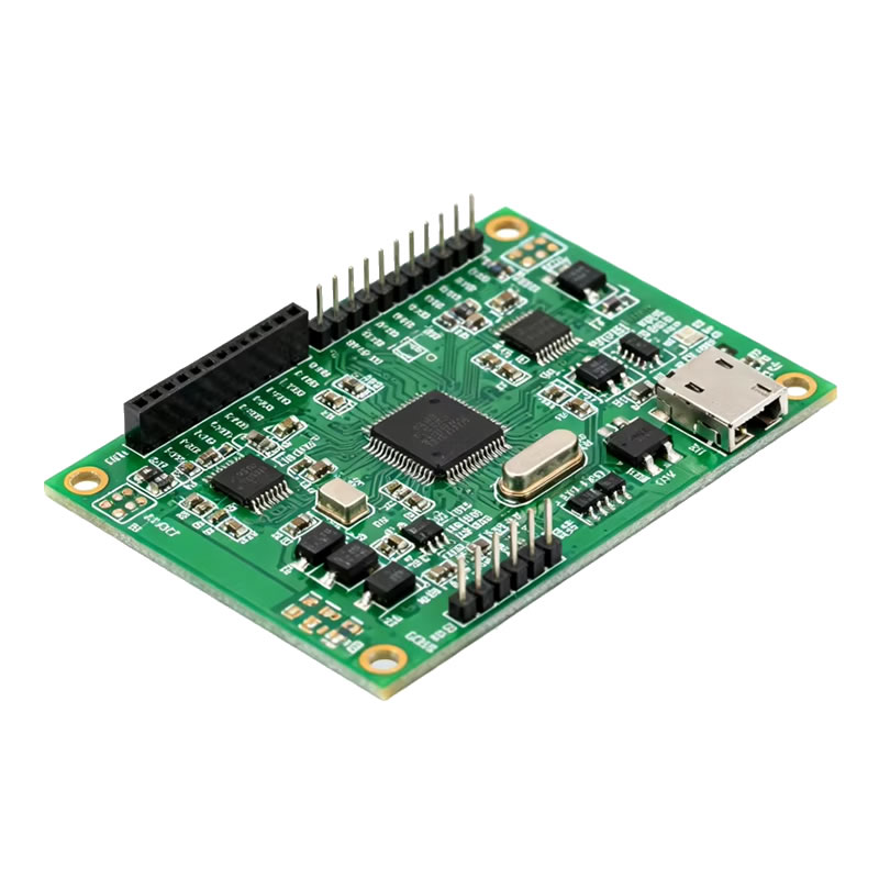
The Internet of Things (IoT) has transformed electronics design. Modern IoT devices – from smart watches and fitness trackers to environmental sensors and home automation hubs – demand compact form factors, low power consumption, and rapid iteration cycles. The IoT Device FR4 PCB is specifically engineered to meet these challenges, balancing high component density with reliable performance in battery-powered, wireless-enabled products.
Key Challenges in IoT PCB Design
IoT devices present unique PCB design challenges that standard boards may not address:
| Challenge | How Our IoT FR4 PCB Solves It |
|---|---|
| Tiny form factor | Fine trace/spacing (4/4 mil minimum) enables dense component placement |
| Mixed signals | Careful stackup separates analog (sensors) from digital (MCU) and RF (wireless) |
| Low power operation | Optimized routing minimizes parasitic capacitance and leakage |
| Wireless integration | Antenna matching and controlled impedance for Bluetooth, WiFi, LoRa, Zigbee |
| Fast iteration | Quick turn prototypes (5-7 days) support agile development |
| Battery compatibility | Low current leakage design extends battery life |
Typical IoT Device Stackup Recommendations
For most IoT devices, we recommend the following stackups based on complexity:
| Device Type | Recommended Layers | Why |
|---|---|---|
| Simple sensor node | 2 layers | Temperature/humidity sensor + battery + wireless module |
| Smart home device | 4 layers | MCU + WiFi/BT + sensors + power management |
| Wearable | 4 or 6 layers | High density, small form factor, battery charging circuit |
| Industrial IoT gateway | 6 or 8 layers | Multiple wireless protocols + processing + I/O |
Technical Specifications for IoT FR4 PCB
| Parameter | Capability |
|---|---|
| Layer count | 2, 4, 6, 8 layers (depending on complexity) |
| Base material | FR4 (Standard or High TG) |
| Board thickness | 0.6mm – 1.6mm (thin boards for wearables) |
| Copper weight | 0.5 oz – 2 oz (1 oz standard for IoT) |
| Min trace width/spacing | 4 mil / 4 mil (0.10mm) – 3 mil available |
| Min drill size | 0.20mm mechanical, 0.10mm laser (for HDI) |
| Controlled impedance | 50Ω (antenna), 90Ω (USB), 100Ω (Ethernet) |
| Surface finish | ENIG recommended – flat surface for fine-pitch components |
| Solder mask | Green, Blue, Black, White, Red |
| Additional services | PCB Assembly (SMT) available – turnkey solution |
Applications for IoT Device FR4 PCB
| Application | Specific Requirements |
|---|---|
| Wearables (watches, bands) | Thin board (0.6-0.8mm), small form factor, battery management |
| Smart home sensors | Low power, wireless (Zigbee/Z-Wave), compact size |
| Environmental monitors | Analog sensor accuracy, long battery life, outdoor durability |
| Medical wearables | High reliability, cleanability, biocompatible considerations |
| Asset trackers | GPS antenna integration, low sleep current, rugged design |
| Smart agriculture sensors | Battery powered, LoRa wireless, moisture/dust resistance |
Why IoT Devices Need Fast Turn PCB Prototypes
IoT product development is iterative by nature. Hardware startups and established companies alike need:
Rapid prototyping – Test a design, measure performance, revise, retest
Short lead times – 5-7 day prototypes keep development on schedule
Low minimum quantities – 5 or 10 pieces for initial validation
Quick design adjustments – Engineering support for last-minute changes
We specialize in fast-turn IoT PCB fabrication, helping you move from concept to production-ready prototype in days, not weeks.
Why Manufacture Your IoT Device FR4 PCB With Us?
| Feature | What You Get for IoT Projects |
|---|---|
| Quick turn prototype | 5-7 days for 2-6 layer IoT boards |
| Mass production | 10-12 days for volume orders |
| Low minimum order | 5 pieces for prototype validation |
| ENIG standard | Best surface finish for fine-pitch IoT components |
| Impedance control | ±10% for antenna matching |
| Assembly available | Turnkey PCB + component sourcing + SMT |
| Engineering support | DFM review focused on IoT design challenges |
Order Process for IoT Device PCB
Upload your Gerber files – specify IoT application type
Receive DFM report with recommendations for compact design
Confirm order – prototype or production quantity
Fabrication – with impedance testing if required
Optional assembly – SMT for your components
Secure shipping with tracking