 PCB & PCBA Manufacturer
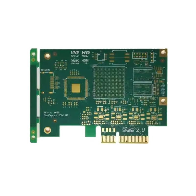
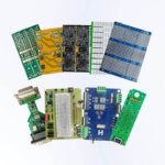
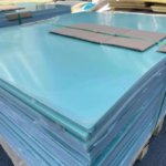
1 Layer to 12 Layer FR4 PCB – Standard & Custom Stackup
Not every PCB requires 12 layers. The right layer count depends on your routing density, signal integrity requirements, EMI sensitivity, and budget.
We manufacture FR4 PCBs from 1 layer to 12 layers, offering both standard stackups (proven, cost-effective) and custom stackups (tailored to your specific impedance, thickness, and performance requirements).
Choose the right layer count for your project – without paying for capabilities you don’t need.
Layer Count Selection Guide
| Layer Count | Common Name | Typical Applications | Key Characteristics |
|---|---|---|---|
| 1 Layer | Single-sided | Remotes, keypads, simple sensors, LED indicators | Lowest cost, components on one side |
| 2 Layer | Double-sided | Most consumer electronics, power supplies, Arduinos | Components both sides, low cost |
| 4 Layer | Multilayer | Industrial controls, IoT devices, automotive modules | Ground + power planes, better EMI |
| 6 Layer | Multilayer | Telecom, networking, medical devices | More routing, better signal integrity |
| 8 Layer | High density | ADAS, high-end industrial, FPGAs | Complex routing, dense BGAs |
| 10 Layer | High density | High-end telecom, servers, advanced computing | Maximum routing density |
| 12 Layer | Very high density | High-speed digital, aerospace, defense | Extreme density, multiple power domains |
What is a Stackup?
A stackup defines the arrangement of copper and insulating layers in a multilayer PCB. It specifies:
| Element | What It Defines |
|---|---|
| Layer order | Which layers are signal, ground, power |
| Dielectric thickness | Distance between copper layers (affects impedance) |
| Copper weight | Thickness of copper on each layer |
| Material type | FR4 grade (Standard TG or High TG 170°C) |
| Total board thickness | Sum of all layers + prepregs + cores |
Standard stackups – Pre-designed, proven arrangements. Lower cost, faster turnaround.
Custom stackups – Designed for your specific impedance, thickness, or performance requirements.
Standard Stackups (Proven & Cost-Effective)
We offer standard stackups for common layer counts. These are pre-optimized for manufacturability and cost:
1 Layer (Single-sided) – Standard Stackup
| Layer | Function | Thickness |
|---|---|---|
| L1 (Top) | Signal + Components | 1 oz copper |
| Substrate | FR4 | 0.6mm – 2.4mm |
| L2 (Bottom) | No copper (single-sided) | – |
2 Layer – Standard Stackup
| Layer | Function | Thickness |
|---|---|---|
| L1 (Top) | Signal + Components | 1 oz copper |
| Substrate | FR4 Core | 1.6mm (typical) |
| L2 (Bottom) | Signal + Components | 1 oz copper |
4 Layer – Standard Stackup (Most Common)
| Layer | Function | Thickness |
|---|---|---|
| L1 (Top) | Signal | 1 oz copper |
| Prepreg | 2116 | ~0.12mm |
| L2 (Ground) | Ground Plane | 1 oz copper |
| Core | FR4 Core | ~1.1mm |
| L3 (Power) | Power Plane | 1 oz copper |
| Prepreg | 2116 | ~0.12mm |
| L4 (Bottom) | Signal | 1 oz copper |
| Total | ~1.6mm |
6 Layer – Standard Stackup
| Layer | Function | Thickness |
|---|---|---|
| L1 (Top) | Signal | 1 oz |
| Prepreg | 1080 | ~0.07mm |
| L2 (Ground) | Ground | 1 oz |
| Core | FR4 Core | ~0.2mm |
| L3 (Signal) | Signal (Inner) | 1 oz |
| Prepreg | 2116 | ~0.12mm |
| L4 (Power) | Power | 1 oz |
| Core | FR4 Core | ~0.8mm |
| L5 (Ground) | Ground | 1 oz |
| Prepreg | 1080 | ~0.07mm |
| L6 (Bottom) | Signal | 1 oz |
| Total | ~1.6mm |
8 Layer / 10 Layer / 12 Layer – Standard Stackups
Available upon request. We provide stackup drawings during DFM review.
Custom Stackups
When standard stackups don’t meet your requirements, we design custom stackups for:
| Requirement | Custom Stackup Solution |
|---|---|
| Controlled impedance (50Ω/90Ω/100Ω) | Adjust dielectric thickness and trace width |
| Specific board thickness (e.g., 1.0mm, 2.0mm) | Custom core/prepreg selection |
| Specific copper weight on inner layers | 2-4 oz on power planes |
| Asymmetric stackups | Different thickness above/below center |
| Blind / buried vias | Additional lamination cycles |
| High TG material (170°C+) | Premium FR4 grade |
We provide custom stackup design free of charge with your order – specify your requirements.
Standard vs. Custom Stackup Comparison
| Feature | Standard Stackup | Custom Stackup |
|---|---|---|
| Design time | None – pre-designed | We design for you (included) |
| Tooling cost | None | None for reasonable volumes |
| Lead time | Fastest (stock materials) | +2-5 days (material selection) |
| Cost | Lowest (standard materials) | +10-30% (non-standard materials) |
| Impedance control | Possible within standard thicknesses | Optimized for your target |
| Best for | Most applications | Impedance control, special thickness |
Recommendation: Use standard stackups unless you have specific impedance or thickness requirements.
1 Layer vs. 2 Layer vs. 4 Layer vs. 6+ Layer – Quick Comparison
| Feature | 1 Layer | 2 Layer | 4 Layer | 6+ Layer |
|---|---|---|---|---|
| Routing layers | 1 | 2 | 2 (with reference planes) | 4+ |
| Ground plane | No (copper pour) | No (copper pour) | Yes – dedicated | Yes – multiple |
| Power distribution | Traces | Traces | Dedicated power plane | Multiple power planes |
| EMI performance | Poor | Poor | Good | Excellent |
| Impedance control | Not recommended | Difficult | Practical | Excellent |
| Component density | Low | Medium | High | Very high |
| Relative cost | Baseline | +20-30% | +50-80% | +100-300% |
| Best for | Simplest products | General purpose | Most commercial products | High-speed, dense designs |
Technical Specifications by Layer Count
| Parameter | 1-2 Layer | 4 Layer | 6 Layer | 8-12 Layer |
|---|---|---|---|---|
| Min trace width | 6 mil (4 mil avail) | 4 mil | 4 mil | 4 mil (3 mil avail) |
| Min drill size | 0.25mm | 0.20mm | 0.20mm | 0.20mm |
| Copper weight | 1-4 oz | 1-4 oz | 1-4 oz | 1-2 oz (inner typical) |
| Board thickness | 0.6-2.4mm | 0.8-2.4mm | 1.0-2.4mm | 1.2-2.4mm |
| Typical lead time (prototype) | 3-5 days | 5-7 days | 7-10 days | 7-12 days |
| Controlled impedance | Not recommended | Yes | Yes | Yes |
| Blind/buried vias | No | No | Limited | Yes |
How to Choose the Right Layer Count
| Question | Answer → Recommended Layers |
|---|---|
| Simple circuit with few components? | → 1 or 2 layer |
| Need good EMI performance? | → 4 layer minimum |
| Have BGA or fine-pitch components? | → 4 layer minimum (6+ for dense BGAs) |
| Need controlled impedance (USB/Ethernet)? | → 4 layer minimum |
| Routing is very tight on 4 layers? | → 6 layer |
| Multiple high-speed interfaces? | → 6 or 8 layer |
| Maximum routing density, many BGAs? | → 8, 10, or 12 layer |
| Cost is primary constraint? | → Lowest possible that works (2 or 4 layer typical) |
Applications by Layer Count
| Layer Count | Typical Applications |
|---|---|
| 1 layer | Remote controls, keypads, simple sensors, LED indicator boards |
| 2 layer | Power supplies, Arduino shields, basic consumer electronics, relay boards |
| 4 layer | Industrial controls, IoT devices, automotive modules, medical monitors |
| 6 layer | Telecom equipment, networking, medical devices, automotive ECUs |
| 8 layer | ADAS, FPGAs, high-end industrial, servers |
| 10-12 layer | High-end telecom, advanced computing, aerospace, defense |
Why Manufacture Your FR4 PCB With Us (1-12 Layers)?
| Feature | What You Get |
|---|---|
| Full range | 1 layer to 12 layers – all in one place |
| Standard stackups | Proven, cost-effective, fast turnaround |
| Custom stackups | Free design for impedance or thickness requirements |
| Free DFM review | We verify stackup works with your design |
| Layer count recommendation | Not sure? We help you choose |
| ISO9001 & UL certified | Quality and safety certified |
| 100% electrical test | Every board tested |
Order Process
Upload Gerber files – specify layer count and stackup (standard or custom)
Free DFM review – we verify stackup compatibility
Stackup drawing provided – for custom stackups
Fabrication – per your specifications
100% electrical test
Secure shipping
Not sure which layer count? Send us your design files and requirements. We recommend the optimal layer count free of charge.