 PCB & PCBA Manufacturer

Heavy Copper FR4 PCB – Up to 6 oz Copper Weight
Standard PCBs use 1 oz copper (approximately 35 µm thick), which can carry about 1-2 amps per 10 mil trace width depending on temperature rise. For high current applications like power supplies, motor drives, battery management systems (BMS), and EV chargers, 1 oz copper requires extremely wide traces or multiple parallel traces, consuming valuable board space and increasing resistance.
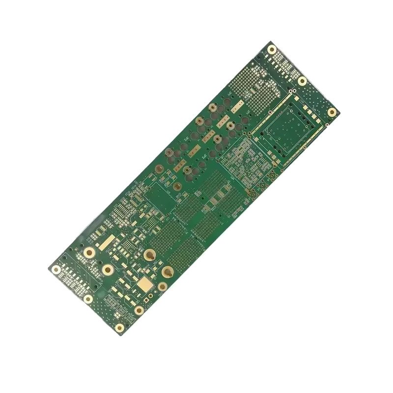
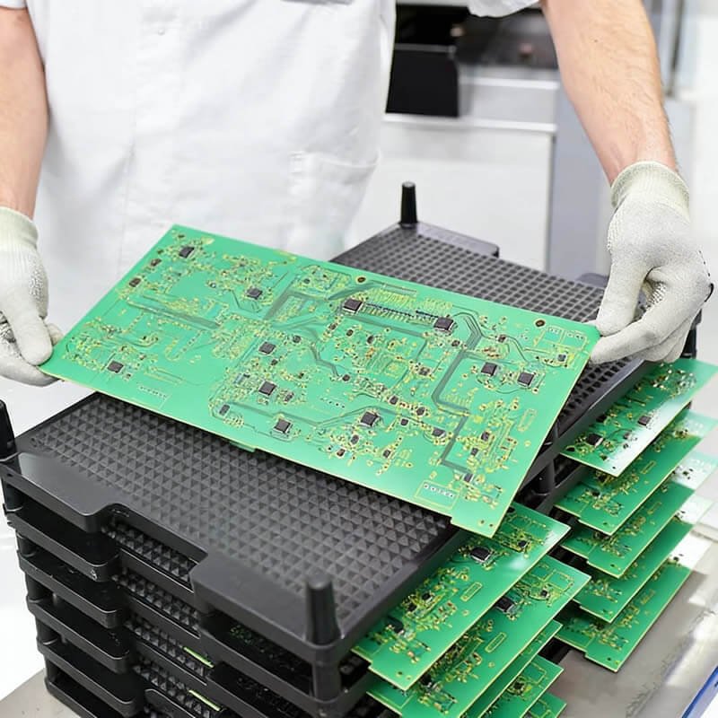
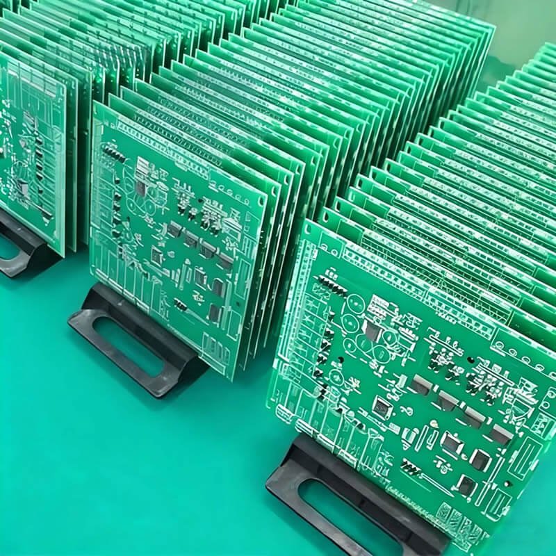
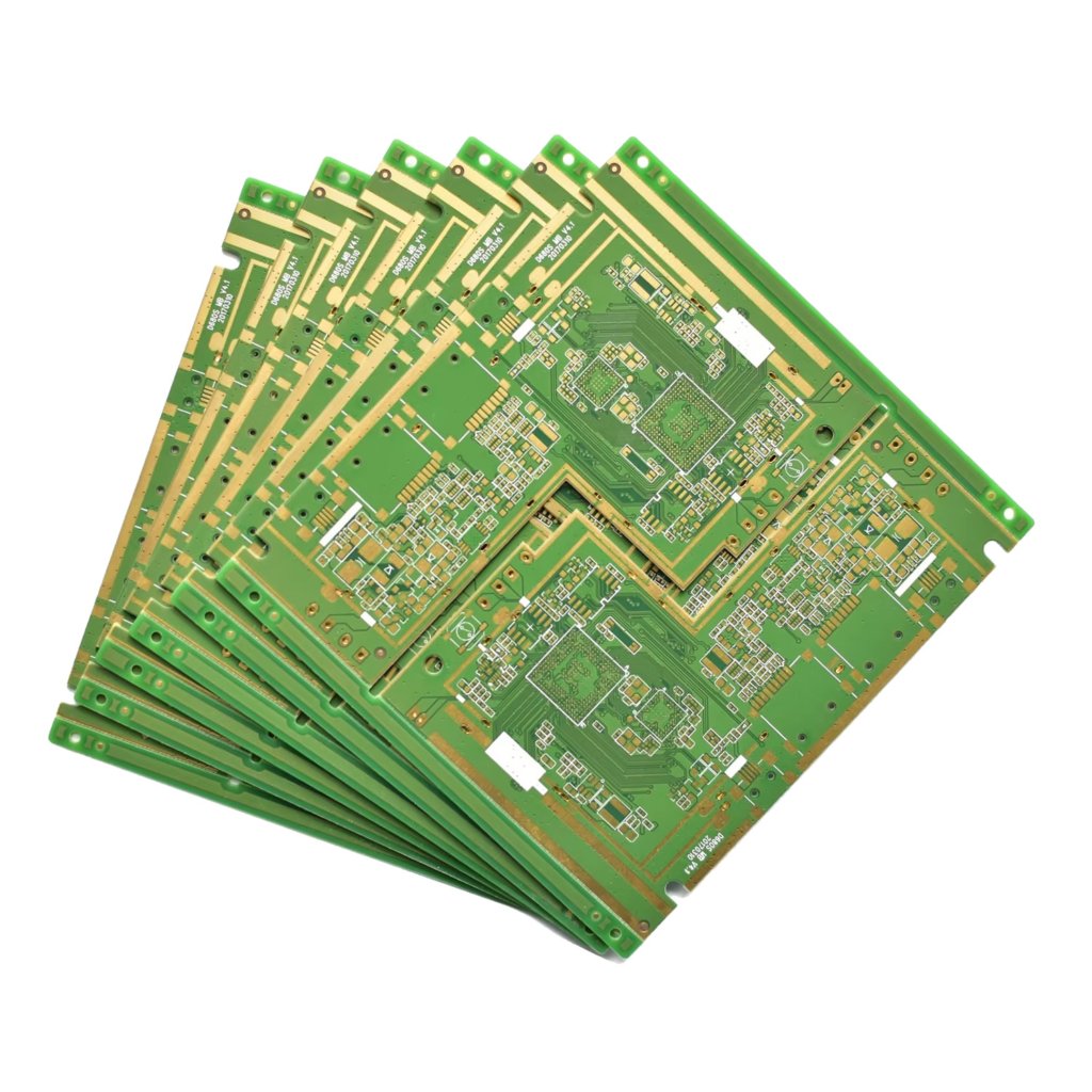
Our Heavy Copper FR4 PCB supports 2 oz to 6 oz copper weight, enabling high current carrying capacity with reduced resistance, lower heat generation, and more efficient board space utilization.
Copper Weight vs. Current Capacity
| Copper Weight | Thickness (µm) | Thickness (mils) | Current Capacity (per 10mm width, 10°C rise) |
|---|---|---|---|
| 1 oz (standard) | 35 µm | 1.4 mil | ~5A |
| 2 oz | 70 µm | 2.8 mil | ~10A |
| 3 oz | 105 µm | 4.2 mil | ~15A |
| 4 oz | 140 µm | 5.6 mil | ~20A |
| 6 oz | 210 µm | 8.4 mil | ~30A |
Note: Current capacity depends on trace width, acceptable temperature rise, and cooling. Wider traces = higher current. Values above are approximate guidelines.
Why Heavy Copper?
| Benefit | Explanation |
|---|---|
| Higher current capacity | 2 oz carries ~2x current of 1 oz for same trace width |
| Lower resistance | Thicker copper = less resistance = less power loss (I²R losses) |
| Less heat generation | Lower resistance = less heat for same current |
| Smaller trace width | 10A requires ~200 mil trace with 1 oz; ~60 mil with 3 oz |
| Better thermal dissipation | Thicker copper spreads heat more effectively |
| Improved reliability | Thicker traces more resistant to damage |
| Inner layer power planes | Distribute high current through internal layers |
Standard vs. Heavy Copper Comparison
| Feature | Standard PCB (1 oz) | Heavy Copper (2-6 oz) |
|---|---|---|
| Current capacity (10mm trace, 10°C rise) | ~5A | ~10-30A (2-6 oz) |
| Trace width for 10A | ~200 mil (5mm) | ~60 mil (1.5mm) with 3 oz |
| Resistance (per square) | ~0.5 mΩ/square | ~0.17 mΩ/square (3 oz) |
| Heat generation (I²R for 10A) | ~0.05W per square | ~0.017W per square (3 oz) |
| Board space efficiency | Poor for high current | Excellent |
| Cost increase vs. 1 oz | Baseline | +30% to +100% |
| Manufacturing lead time | Standard | +2-5 days |
| Best for | Signal, low power | Power supplies, motor drives, BMS, EV |
Copper Weight Selection Guide
| Application | Recommended Copper Weight | Typical Current |
|---|---|---|
| Low power supply (<5A) | 1 oz (standard) | <5A |
| Medium power supply (5-10A) | 2 oz | 5-10A |
| High power supply (10-15A) | 3 oz | 10-15A |
| Motor drive (15-20A) | 4 oz | 15-20A |
| Battery management (20-30A) | 6 oz | 20-30A |
| EV charger / industrial (>30A) | 6+ oz or bus bars | >30A |
Technical Specifications for Heavy Copper FR4 PCB
| Parameter | Capability |
|---|---|
| Copper weight (outer layers) | 2 oz, 3 oz, 4 oz, up to 6 oz |
| Copper weight (inner layers) | 2 oz, 3 oz, 4 oz, up to 6 oz |
| Layer count | 2 to 8+ layers |
| Base material | High TG FR4 (TG 170°C) – recommended for heavy copper |
| Board thickness | 1.0mm – 3.2mm (thicker for heavy copper) |
| Min trace width (power traces) | No minimum – as wide as needed |
| Min trace width (signal traces) | 6-8 mil (heavy copper etching limits fine traces) |
| Min spacing | 8-10 mil (for heavy copper layers) |
| Surface finish | ENIG (preferred), HASL Lead-Free, OSP |
| Thermal management | Thermal vias, copper pours, heat sink mounting |
| Inspection | 100% AOI + electrical test |
Important Note on Trace Width and Spacing for Heavy Copper
Heavy copper requires larger minimum trace width and spacing than standard 1 oz copper due to etching limitations:
| Copper Weight | Min Trace / Spacing (Outer Layers) |
|---|---|
| 1 oz (standard) | 4 mil / 4 mil |
| 2 oz | 6 mil / 6 mil |
| 3 oz | 8 mil / 8 mil |
| 4 oz | 10 mil / 10 mil |
| 6 oz | 12 mil / 12 mil |
For power traces (carrying high current), use wide traces (no minimum – as wide as needed). For signal traces on heavy copper boards, use separate thinner copper layers (standard 1 oz) if fine traces are needed.
Applications for Heavy Copper FR4 PCB
| Application | Recommended Copper | Why |
|---|---|---|
| AC-DC power supplies | 2-3 oz | High current output stages |
| DC-DC converters | 2-4 oz | Switching currents, power planes |
| Battery management systems (BMS) | 3-6 oz | High charge/discharge currents |
| Motor drives (Brushed/BLDC) | 4-6 oz | High inrush currents, continuous operation |
| EV chargers (on-board) | 4-6 oz | 20-50A charging currents |
| Servo drives / industrial VFDs | 4-6 oz | High power, reliability |
| Power inverters (solar, UPS) | 3-4 oz | AC power switching |
| LED lighting (high power) | 2-3 oz | High current LED strings |
| Welding equipment | 6+ oz | Extreme currents (100A+) – may require bus bars |
| Electric vehicle (traction) | 6+ oz | 50-100A+ – typically bus bars |
Thermal Management for Heavy Copper PCBs
Heavy copper carries high current, which generates heat. Proper thermal management is essential:
| Thermal Feature | Purpose |
|---|---|
| Wide power traces | Minimize resistance (I²R heating) |
| Copper pours (planes) | Spread heat across larger area |
| Thermal vias | Conduct heat from top-layer components to inner/back layers |
| High TG material (170°C+) | Maintain mechanical stability at elevated temperatures |
| Heat sink mounting holes | Attach external heat sinks to power components |
| Conformal coating (optional) | Not for thermal – protects from environment |
Can Heavy Copper Be Used on Inner Layers?
Yes. Heavy copper can be applied to inner layers as well as outer layers:
| Location | Benefit |
|---|---|
| Outer layers | Connect to power components (MOSFETs, inductors, connectors) |
| Inner layers | Power planes distributing current across board without using outer layer space |
Stackup example (4-layer with heavy copper inner planes):
L1: 2 oz (component side, power traces)
L2: 4 oz (inner power plane, high current distribution)
L3: 4 oz (inner ground plane, return path)
L4: 2 oz (bottom side, secondary components)
This approach keeps outer layer routing easy while inner layers handle high current distribution.
Heavy Copper vs. Bus Bars
| Feature | Heavy Copper (4-6 oz) | Bus Bars (metal bars) |
|---|---|---|
| Current capacity | Up to ~30-40A (6 oz, wide traces) | 50A to 500A+ |
| PCB integration | Directly on PCB – no separate part | Requires assembly (screws, soldering) |
| Space required | Low – traces on PCB | High – separate bars |
| Cost | Medium (included in PCB cost) | High (fabrication + assembly) |
| Best for | Up to 30-40A continuous | >40A, very high current |
Recommendation: For currents up to 30-40A, heavy copper (4-6 oz) is cost-effective and space-efficient. For higher currents, consider bus bars or hybrid approach.
Why Manufacture Your Heavy Copper FR4 PCB With Us?
| Feature | What You Get |
|---|---|
| Heavy copper up to 6 oz | 2 oz, 3 oz, 4 oz, 6 oz – inner and outer layers |
| High TG material standard | TG 170°C recommended for thermal stability |
| Detailed stackup design | We help design layer stackup with heavy copper planes |
| 100% electrical test | Including high current path verification |
| Engineering support | DFM review for heavy copper design rules |
| Automotive & industrial experience | BMS, motor drives, EV chargers |
| ISO9001 certified | Full quality management |
Order Process for Heavy Copper FR4 PCB
Upload Gerber files – specify copper weight (2/3/4/6 oz), inner/outer or both
Receive DFM report – verify trace/spacing for heavy copper
Stackup design – we recommend layer stackup with heavy copper planes
Fabrication – heavy copper process (additional plating/etching cycles)
100% electrical test – including high current path verification
Secure shipping