 PCB & PCBA Manufacturer

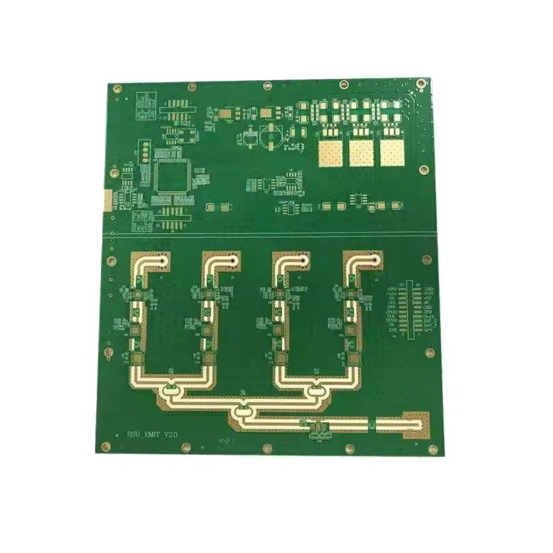

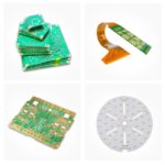
Controlled Impedance FR4 PCB – 50Ω / 90Ω / 100Ω
Modern high-speed digital and RF designs require precise impedance control to maintain signal integrity. Without controlled impedance, reflections occur, data becomes corrupted, EMI increases, and products fail certification.
Our Controlled Impedance FR4 PCB supports the three most common industry-standard impedances:
| Impedance | Type | Common Applications |
|---|---|---|
| 50Ω | Single-ended | GPS, Cellular (4G/5G), Bluetooth, WiFi, RF antennas |
| 90Ω | Differential | USB 2.0, USB 3.0/3.1, LVDS (Low-Voltage Differential Signaling), Camera interfaces |
| 100Ω | Differential | Ethernet (100BASE-T, 1000BASE-T), HDMI, DisplayPort, PROFINET |
Why Controlled Impedance Matters
| Problem Without Impedance Control | Consequence |
|---|---|
| Signal reflections | Data errors, corrupted communication |
| Overshoot / ringing | Potential damage to ICs |
| EMI / radiated emissions | FCC/CE certification failure |
| Reduced noise margin | Intermittent failures, field returns |
| Poor eye diagram opening | Limited cable length, unstable links |
Controlled impedance ensures consistent characteristic impedance along each trace, matching driver and receiver, thereby minimizing reflections and maintaining signal integrity.
How Impedance is Controlled on FR4
Impedance on FR4 is determined by four key parameters:
| Parameter | Impact on Impedance | Controlled By |
|---|---|---|
| Trace width (W) | Wider = lower impedance | PCB layout (Gerber) |
| Trace spacing (S) | Wider spacing (differential) = higher impedance | PCB layout (Gerber) |
| Dielectric thickness (H) | Thicker dielectric = higher impedance | PCB stackup (layer thickness) |
| Dielectric constant (Dk) | Higher Dk = lower impedance | FR4 material selection (Dk ~4.2-4.6) |
How we achieve your target impedance:
You specify target impedance (50Ω, 90Ω, 100Ω) and tolerance
We recommend copper weight, layer thickness (prepreg/core), and stackup
We calculate trace width (and spacing for differential) for your specific stackup
We fabricate with process controls (etching, lamination) maintaining ±10% tolerance
Optional TDR testing – verify impedance on finished boards
Standard Impedance Specifications
| Parameter | Standard Capability | Advanced Capability |
|---|---|---|
| 50Ω single-ended | ±10% | ±8% or ±5% |
| 90Ω differential | ±10% | ±8% or ±5% |
| 100Ω differential | ±10% | ±8% or ±5% |
| Custom impedance | ±10% | ±8% or ±5% |
| Test method | TDR (Time Domain Reflectometry) or impedance coupons | Same |
| Documentation | Impedance test report included | Same |
Note: Tighter tolerance (±5% or ±8%) may require additional process controls and testing – please inquire.
Impedance Test Structures (Coupons)
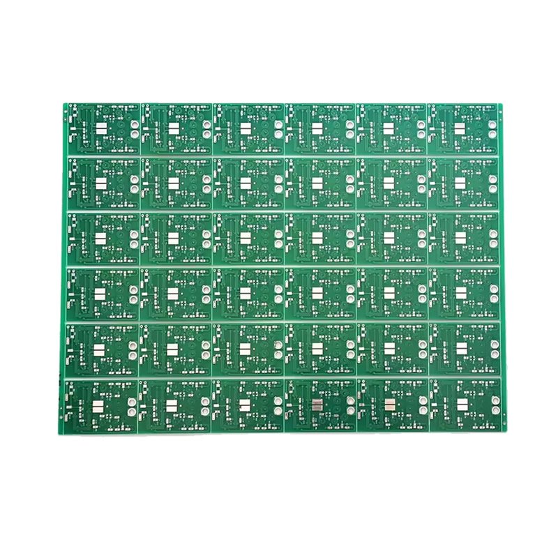
We include impedance test coupons on each production panel:
| Coupon Type | Placement | Purpose |
|---|---|---|
| 50Ω coupon | Panel edge or customer-defined location | Verify single-ended impedance |
| 90Ω coupon | Panel edge or customer-defined location | Verify USB/LVDS differential impedance |
| 100Ω coupon | Panel edge or customer-defined location | Verify Ethernet/HDMI differential impedance |
For prototype orders with single pieces (no panel): We can include impedance coupons on an additional small board or use similar panel data.
Impedance test report included with each controlled impedance order.
Layer Stackup Recommendations
| Board Complexity | Recommended Stackup | Impedance Layers |
|---|---|---|
| 2-layer | Not recommended (no ground plane reference) | Avoid – inconsistent results |
| 4-layer | Top (Signal) / Ground / Power / Bottom (Signal) | Top layer (L1) referenced to L2 ground |
| 6-layer | Top / Ground / Signal / Power / Ground / Bottom | L1 to L2 ground, L3 to L4 power, L6 to L5 ground |
| 8+ layers | Multiple signal + ground layers | Various reference planes |
Minimum recommendation: 4-layer PCB with signal layer adjacent to ground plane for consistent impedance.
2-layer boards: Impedance control is possible but not recommended due to inconsistent reference (copper pour vs. no pour). We recommend 4+ layers for controlled impedance.
Technical Specifications for Controlled Impedance FR4 PCB
| Parameter | Capability |
|---|---|
| Supported impedances | 50Ω, 90Ω, 100Ω (custom available) |
| Tolerance standard | ±10% (industry standard) |
| Tolerance advanced | ±8% or ±5% (on request) |
| Test method | TDR (Time Domain Reflectometry) |
| Test coupons | Included on production panels |
| Layer count | 4+ layers recommended (2-layer possible but not recommended) |
| Base material | FR4 (Standard or High TG) |
| Dielectric constant (Dk) | 4.2-4.6 (frequency dependent) |
| Trace width/spacing (for impedance) | Calculated per stackup (typically 4-8 mil) |
| Surface finish | ENIG preferred (flat surface, consistent Dk) |
| Documentation | Impedance test report included |
Applications Requiring Controlled Impedance
| Application | Impedance | Why Required |
|---|---|---|
| GPS receiver | 50Ω | Antenna matching – satellite signal integrity |
| Cellular module (4G/5G) | 50Ω | RF performance, radiated power, sensitivity |
| Bluetooth / WiFi | 50Ω | Antenna matching – range and throughput |
| USB 2.0 | 90Ω differential | Data integrity up to 480 Mbps |
| USB 3.0/3.1 | 90Ω differential | 5-10 Gbps – extremely sensitive |
| LVDS (camera, display) | 90Ω or 100Ω differential | Video data integrity |
| Ethernet (100BASE-T) | 100Ω differential | Network reliability |
| Gigabit Ethernet (1000BASE-T) | 100Ω differential | 1 Gbps – requires tight control |
| HDMI / DisplayPort | 100Ω differential | Video/audio integrity |
| Automotive radar (ADAS) | 50Ω | Safety-critical signal integrity |
Standard FR4 vs. Controlled Impedance
| Feature | Standard FR4 PCB | Controlled Impedance FR4 PCB |
|---|---|---|
| Impedance tolerance | Uncontrolled (±20-30% or more) | Controlled (±10% standard) |
| Trace width design | Rule-of-thumb (e.g., 10 mil) | Calculated from stackup |
| Stackup design | Standard (e.g., 1.6mm total) | Customized for impedance |
| Test coupons | Not included | Included on panel |
| Impedance testing | None | TDR test + report |
| Documentation | COC only | Impedance test report included |
| Best for | Low-speed, non-critical signals | High-speed, RF, USB, Ethernet, HDMI |
| Cost | Baseline | +15-30% (coupons + testing + engineering) |
| Lead time | Standard | +1-3 days (test coupon design) |
Impedance Tolerance Comparison
| Tolerance | Difficulty | Cost Impact | Typical Applications |
|---|---|---|---|
| ±15% | Easy | Minimal | Non-critical high-speed |
| ±10% | Standard | Baseline (+15-30% vs. non-controlled) | USB 2.0, 100Mb Ethernet |
| ±8% | Moderate | +5-10% vs. ±10% | USB 3.0, Gigabit Ethernet |
| ±5% | Difficult | +15-25% vs. ±10% | High-speed (>5 Gbps), RF precision |
Industry standard: ±10% – sufficient for most applications including USB 2.0, 100Mb Ethernet, Bluetooth/WiFi.
TDR (Time Domain Reflectometry) Testing
TDR is the industry-standard method for verifying impedance:
| Aspect | Description |
|---|---|
| How it works | Sends fast rise-time pulse down the trace, measures reflected energy |
| What it measures | Characteristic impedance along entire trace length |
| Output | Impedance vs. distance graph + pass/fail determination |
| Defects detected | Opens, shorts, impedance discontinuities (connectors, vias, corners) |
We provide TDR test reports showing measured impedance values with min/max/average.
High-Speed Design Recommendations
For best impedance control results:
| Recommendation | Why |
|---|---|
| 4+ layers minimum | Signal layer adjacent to ground plane |
| Use ground planes, not grids | Solid copper provides consistent reference |
| Avoid splitting reference plane under signals | Causes impedance discontinuities |
| Maintain consistent dielectric thickness | Use standard prepreg/core thicknesses |
| Avoid 90° corners | Use 45° or rounded corners |
| Keep differential pairs length-matched | Within 5-10 mils (0.13-0.25mm) |
| Maintain consistent trace spacing | No necking or widening |
| Minimize via count | Each via adds impedance discontinuity |
| Remove unused pads from inner layers | Reduces capacitive loading |
Submit your design for free DFM review with impedance control recommendations.
Why Manufacture Your Controlled Impedance FR4 PCB With Us?
| Feature | What You Get |
|---|---|
| Standard ±10% tolerance | Suitable for most high-speed applications |
| Tighter tolerance available | ±8% or ±5% on request |
| TDR testing | Verification with test report included |
| Impedance coupons | Included on production panels |
| Custom stackup design | We calculate trace width/spacing for your target impedance |
| Free engineering support | DFM review with impedance recommendations |
| 4+ layer capability | Up to 12+ layers (2-layer possible but not recommended) |
| 100% electrical test | Plus impedance test coupons |
Order Process for Controlled Impedance FR4 PCB
Upload Gerber files – specify target impedance(s), tolerance, and which layers
Free stackup design – we calculate trace width/spacing, recommend materials
Review and approve stackup + test coupon location
Fabrication – with process controls for impedance
TDR testing – verify impedance on coupons (or actual traces on request)
Impedance test report – included with shipment
Secure shipping