 PCB & PCBA Manufacturer
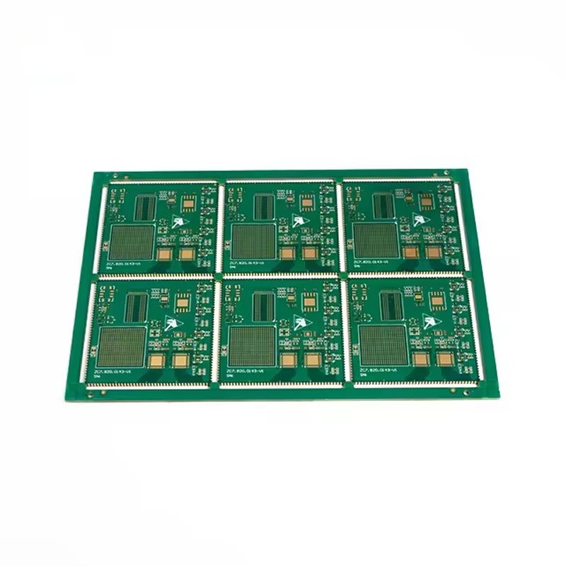
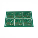
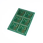
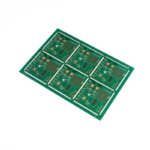
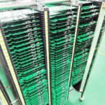
6 Layer FR4 PCB – More Routing Space & Better EMI Control
When a 4-layer PCB reaches its limits in routing density or signal integrity, the 6 Layer FR4 PCB is the logical next step. It offers two additional routing layers and improved EMI shielding without the complexity or cost of an 8-layer board. For many industrial, automotive, and telecom applications, 6 layers represent the sweet spot between performance and manufacturability.
Why Upgrade from 4-Layer to 6 Layer FR4 PCB?
A standard 4-layer board typically follows a simple stackup: Top Signal, Ground, Power, Bottom Signal. This leaves no room for internal signal routing, forcing all traces to the outer layers. A 6 layer stackup solves this problem:
| Limitation of 4-Layer | Solution with 6 Layer FR4 PCB |
|---|---|
| All signals on outer layers – limited routing channels | Two internal signal layers free up outer layers for components |
| Power and ground share limited planes | Dedicated power plane + dedicated ground plane – cleaner power delivery |
| Longer return paths – more EMI radiation | Adjacent ground planes provide short return paths – lower EMI |
| Difficulty mixing analog & digital signals | Separate internal layers for sensitive vs. noisy signals |
Typical Layer Stackup for 6 Layer FR4 PCB
| Layer | Function | Purpose |
|---|---|---|
| Layer 1 | Top Signal | Component placement & critical traces |
| Layer 2 | Ground | Reference plane, short return path |
| Layer 3 | Signal (Inner 1) | High-speed or sensitive routing |
| Layer 4 | Power | Core voltage distribution |
| Layer 5 | Ground | Reference plane, shielding |
| Layer 6 | Bottom Signal | Secondary components & routing |
This asymmetrical stackup is common and cost-effective. For applications requiring perfect symmetry to prevent warpage, we can recommend alternative stackups.
Technical Specifications
| Parameter | Capability |
|---|---|
| Layer count | 6 layers (4, 8, 10, 12 layers also available) |
| Base material | FR4 (TG 130°C – 170°C) |
| Board thickness | 0.8mm – 2.4mm (customizable) |
| Copper weight | 1 oz – 3 oz (inner & outer) |
| Min trace width/spacing | 4 mil / 4 mil (0.10mm) |
| Min annular ring | 4 mil |
| Min mechanical drill | 0.20mm |
| Surface finish | HASL Lead-Free, ENIG, OSP, Immersion Silver |
| Solder mask color | Green, Blue, Red, Black, White, Yellow |
| Silkscreen color | White, Black, Yellow |
Applications for 6 Layer FR4 PCB
| Application | Why 6 Layers? |
|---|---|
| Industrial sensors & controllers | Mixed analog/digital signals need separation |
| Automotive ECUs (non-safety) | Better EMI immunity in electrically noisy environments |
| Telecom access equipment | Multiple interfaces requiring ground isolation |
| Medical monitoring devices | Compact form factor + power integrity |
| Consumer electronics mid-tier | Cost-effective upgrade from 4-layer for better performance |
| Battery management systems (BMS) | Dedicated power plane for current sensing circuits |
4-Layer vs. 6 Layer FR4 PCB – Quick Comparison
| Feature | 4-Layer PCB | 6 Layer FR4 PCB |
|---|---|---|
| Routing layers | 2 (top + bottom) | 4 (top + bottom + 2 internal) |
| Signal density | Low to medium | Medium to high |
| EMI performance | Basic | Significantly better |
| Power distribution | Shared ground/power planes | Dedicated power plane |
| Cost | Baseline | +25% to 35% |
| Best for | Simple consumer, basic controls | Industrial, automotive, telecom |
Why Manufacture Your 6 Layer FR4 PCB With Us?
| Feature | What You Get |
|---|---|
| Quick turn prototype | 5-7 days for 6 layer prototypes |
| Mass production | 10-12 days for volume orders |
| Impedance control | ±10% (tighter on request) |
| AOI + Flying Probe | 100% electrical testing before shipment |
| UL & ISO9001 certified | Full traceability and quality system |
| Engineering support | DFM review before production – free of charge |
Order Process
Upload your Gerber files and stackup requirements
Receive engineering review and DFM report
Confirm order and proceed to fabrication
100% electrical test before packaging
Secure shipping with tracking