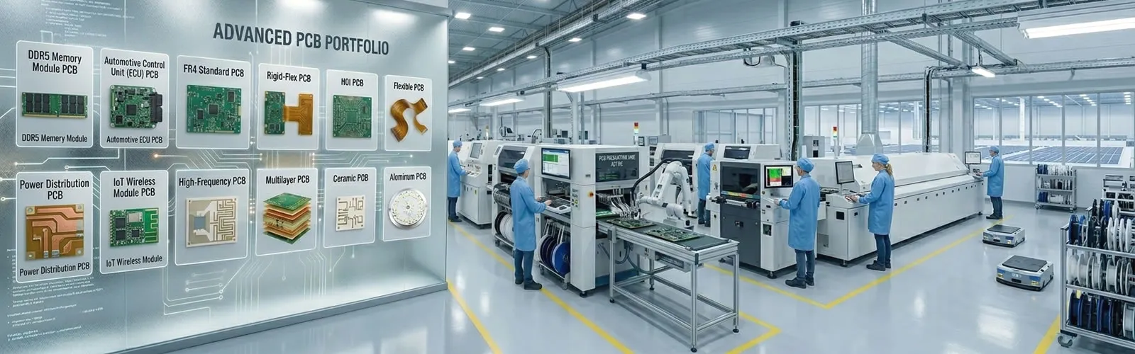
Flex PCB – Flex Circuit Board Fabrication
Flex PCB (flexible printed circuit board) fabrication is the process of manufacturing thin, bendable circuit boards using polyimide as the base material instead of rigid FR4.
Unlike rigid PCBs that crack under stress, flex PCBs are designed to bend, fold, and twist – making them ideal for wearable devices, medical equipment, aerospace systems, and any application where space is limited or movement is required.
As a specialized flex circuit board fabrication house, we produce custom flexible PCBs from 1 to 6 layers (8 on request) with RA copper standard, polyimide coverlay, and optional stiffeners for component support.
What is Flex PCB Fabrication?
| Feature | Rigid PCB Fabrication | Flex PCB Fabrication |
|---|---|---|
| Base material | FR4 (glass epoxy) | Polyimide (Kapton) |
| Finished thickness | 0.6mm – 2.4mm | 0.1mm – 0.4mm |
| Copper type | ED copper (standard) | RA copper (rolled annealed) |
| Surface protection | Solder mask (brittle) | Coverlay (polyimide – flexible) |
| Bendability | None | Yes – designed to bend |
| Typical layer count | 1-12+ layers | 1-6 layers (8 on request) |
Flex PCB Fabrication Process
| Step | What Happens | Key Difference vs. Rigid |
|---|---|---|
| 1. Material preparation | Polyimide base + RA copper laminate | Flexible material requires handling |
| 2. Circuit imaging | Photoresist applied, traces exposed | Similar to rigid but thinner material |
| 3. Etching | Remove unwanted copper | RA copper etches differently |
| 4. Coverlay application | Polyimide film with adhesive applied | Coverlay not solder mask |
| 5. Lamination | Heat and pressure to bond layers | Lower temperature for polyimide |
| 6. Drilling | Mechanical or laser drilling | Laser for microvias (optional) |
| 7. Plating | Copper plating for vias | Similar to rigid |
| 8. Surface finish | ENIG, Immersion Silver, etc. | Same options as rigid |
| 9. Stiffener attachment | FR4, polyimide, or metal (optional) | Unique to flex |
| 10. Routing / cutting | Laser or die-cutting | Laser for precision |
| 11. Electrical test | 100% continuity, isolation | Similar to rigid |
Flex PCB Fabrication – Capabilities
| Parameter | Our Fabrication Capability |
|---|---|
| Layer count | 1 to 6 layers (8 on request) |
| Board thickness (no stiffener) | 0.1mm to 0.4mm |
| Board thickness (with stiffener) | 0.2mm to 0.6mm |
| Copper weight | 0.5 oz or 1 oz |
| Copper type | RA copper standard |
| Min trace width/spacing | 3 mil / 3 mil (2 mil available) |
| Min drill size (mechanical) | 0.15mm |
| Min drill size (laser) | 0.10mm (microvia) |
| Min coverlay opening | 0.2mm |
| Max board size | 250mm x 600mm |
| Stiffener materials | FR4, polyimide, aluminum, steel |
| Stiffener thickness | 0.05mm to 0.5mm |
| Surface finishes | ENIG, HASL, Immersion Silver, OSP, Hard Gold |
| Coverlay colors | Yellow, black, white |
Why RA Copper is Standard in Flex Fabrication
| Copper Type | Grain Structure | Flex Life | Our Use |
|---|---|---|---|
| RA copper (rolled annealed) | Horizontal grains | Excellent (10,000+ cycles) | Standard |
| ED copper (electro-deposited) | Columnar grains | Poor (100-1,000 cycles) | Static flex only |
RA copper is manufactured by rolling – aligning grain structure horizontally, making it more resistant to cracking under repeated bending. We use RA copper as standard for all flex PCB fabrication.
Coverlay vs. Solder Mask – Critical Difference
| Feature | Solder Mask (Rigid) | Coverlay (Flex) |
|---|---|---|
| Material | Liquid photoimageable ink | Polyimide film with adhesive |
| Flexibility | Brittle – cracks when bent | Flexible – bends with board |
| Thickness | 0.5-1 mil | 0.5-1 mil (similar) |
| Application | Screen printing or spray | Lamination with heat/pressure |
| Best for | Rigid PCBs | Flex PCBs |
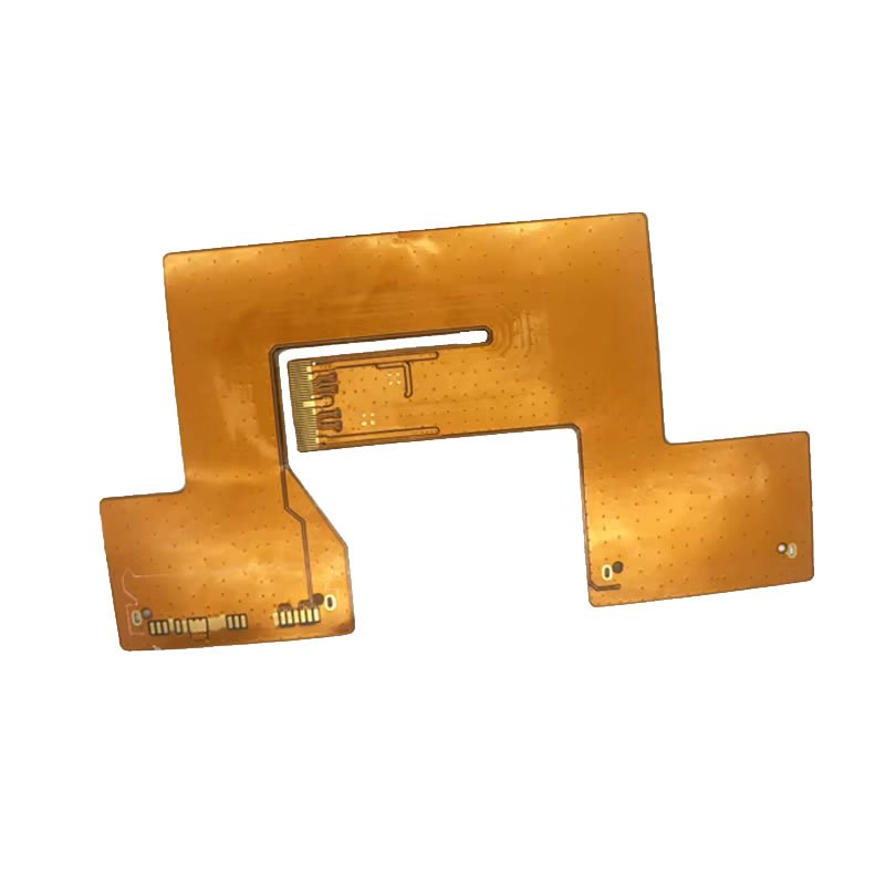
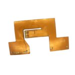
We use polyimide coverlay (not solder mask) on all flex PCB fabrication – it bends without cracking.
Flex PCB Fabrication – Design for Manufacturing (DFM) Guidelines
| Design Element | Recommendation | Why |
|---|---|---|
| Bend radius (static) | ≥10x flex thickness | Prevents copper fatigue |
| Bend radius (dynamic) | ≥30x flex thickness | For repeated bending (hinges) |
| Trace direction | Perpendicular to bend axis | Minimizes stress on traces |
| Via placement | No vias in bend areas | Vias crack under flex stress |
| Copper weight | 0.5 oz preferred | Thinner copper bends better |
| Coverlay openings | ≥0.2mm from copper edge | Prevents shorting |
| Stiffener placement | Outside bend areas | Prevents stress concentration |
| Annular ring | ≥4 mil | Prevents via breakout |
| Trace corners | 45° or rounded (not 90°) | Reduces stress concentration |
Common Flex PCB Fabrication Configurations
| Configuration | Layer Count | Total Thickness | Typical Application |
|---|---|---|---|
| Single layer (1L) | 1 copper layer | 0.1-0.15mm | Simple flex, wearables, sensors |
| Double layer (2L) | 2 copper layers | 0.15-0.2mm | Standard FPC, most applications |
| Multilayer (4L) | 4 copper layers | 0.3-0.4mm | Complex circuits, medical devices |
| Multilayer (6L) | 6 copper layers | 0.4-0.5mm | High-density, aerospace |
| With stiffeners | Any + stiffeners | +0.1-0.5mm | Component support, ZIF connectors |
Applications for Flex PCB Fabrication
| Industry | Typical Applications | Fabrication Requirements |
|---|---|---|
| Wearables | Smartwatches, fitness bands, hearing aids | Ultra-thin (0.1mm), RA copper |
| Medical | Endoscopes, patient monitors, sensors | High reliability, coverlay protection |
| Aerospace | Avionics, satellite harnesses | Lightweight, high reliability |
| Automotive | Sensors, lighting, battery management | Temperature range, vibration |
| Industrial | Robotics, sensors, dynamic cabling | Dynamic flex, rugged |
| Consumer | Smartphones, foldable phones, cameras | Fine pitch, high volume |
| Defense | Portable radios, ruggedized equipment | MIL-spec, shock resistance |
Flex PCB Fabrication vs. Rigid PCB Fabrication – Cost & Lead Time
| Aspect | Rigid PCB | Flex PCB |
|---|---|---|
| Material cost | Lower (FR4) | Higher (polyimide) |
| Processing cost | Lower | Higher (specialized processes) |
| Tooling / setup | Standard | Similar (may be higher for flex) |
| Lead time (prototype) | 3-7 days | 7-10 days |
| Lead time (production) | 7-12 days | 10-15 days |
| Per-board cost (low volume) | Lower | Higher |
| Per-board cost (high volume) | Low | Moderate (gap narrows) |
Why Choose Our Flex PCB Fabrication?
| Feature | What You Get |
|---|---|
| Specialized flex fabrication | Flex is our core competency |
| RA copper standard | No upcharge – always included |
| Coverlay (not solder mask) | Flexible protection – won’t crack |
| Free DFM review | Flex-specific check included |
| No MOQ for prototypes | Order as few as 5 pieces |
| Fast turnaround | Prototypes in 7-10 days |
| Stiffeners available | FR4, polyimide, metal |
| ISO9001 & UL certified | Quality guaranteed |
Order Process for Flex PCB Fabrication
Send your Gerber files – specify layer count, thickness, stiffener requirements
Free DFM review – flex-specific check (24 hours)
Receive quotation – detailed pricing
Order first article (5-20 pieces) – recommended for validation
Fabrication – built to your specifications
100% electrical test
Secure shipping – worldwide delivery
Need flex PCB fabrication? We specialize in flexible circuits. Send your Gerber files for a free DFM review and quote.


