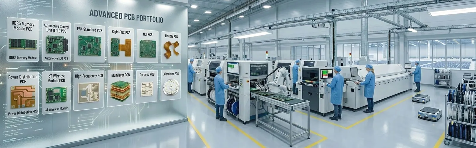
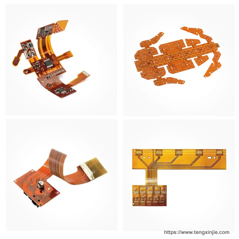
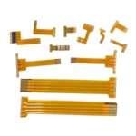
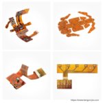
Flex PCBs – High-Density Flexible PCB Manufacturing
As electronic devices become smaller, thinner, and more feature-rich, the demand for high-density flexible PCBs continues to grow. Standard flex PCBs with 1-2 layers and 6/6 mil trace/space are no longer sufficient for today’s compact designs.
Our high-density flex PCB manufacturing capabilities include fine-pitch traces (3/3 mil) , multi-layer flexible construction (up to 6 layers) , and microvias (0.10mm laser drilled) – enabling you to pack more functionality into less space.
What is High-Density Flex PCB?
| Feature | Standard Flex PCB | High-Density Flex PCB |
|---|---|---|
| Trace width/spacing | 6/6 mil or larger | 3/3 mil or finer |
| Layer count | 1-2 layers | 4-6 layers (up to 8 on request) |
| Via size | 0.20mm mechanical | 0.10mm laser microvias |
| Component density | Low to medium | High to very high |
| Board thickness | 0.15-0.3mm | 0.2-0.5mm (more layers) |
| Typical applications | Simple flex, sensors | Smartphones, wearables, medical |
High-Density Flex PCB Capabilities
| Parameter | Our Capability |
|---|---|
| Layer count | 1 to 6 layers (8 layers on request) |
| Min trace width/spacing | 3 mil / 3 mil (0.075mm) – 2 mil available |
| Min drill size (mechanical) | 0.15mm |
| Min drill size (laser) | 0.10mm (microvia) |
| Copper weight | 0.5 oz or 1 oz (RA copper standard) |
| Board thickness (1-2 layer) | 0.1mm – 0.2mm |
| Board thickness (4-6 layer) | 0.3mm – 0.5mm |
| Min coverlay opening | 0.2mm |
| Surface finish | ENIG (preferred), Immersion Silver, OSP |
| Stiffeners | FR4, polyimide, metal |
| EMI shielding | Silver ink, copper layer, shielding film |
High-Density Flex – Design Considerations
| Design Element | High-Density Recommendation | Why |
|---|---|---|
| Trace width/spacing | 3/3 mil minimum | Enables higher routing density |
| Via type | Laser microvias (0.10mm) | Saves space vs. mechanical vias |
| Via placement | Avoid bend areas | Vias crack under flex stress |
| Copper weight | 0.5 oz preferred | Thinner copper = finer traces |
| Layer count | 4-6 layers for complex routing | Distributes signals efficiently |
| Stackup symmetry | Balanced construction | Prevents warpage |
| Component placement | Rigid sections or stiffener areas | Flex too thin for heavy parts |
High-Density Flex – Layer Stackup Examples
4-Layer High-Density Flex Stackup
| Layer | Material | Thickness | Function |
|---|---|---|---|
| Coverlay | Polyimide | 0.5 mil | Protection |
| L1 (Copper) | RA copper, 0.5 oz | 0.7 mil | Signal / component |
| Adhesive | Acrylic | 0.5 mil | Bonding |
| Polyimide core | DuPont Kapton | 1 mil | Insulation |
| L2 (Copper) | RA copper, 0.5 oz | 0.7 mil | Ground plane |
| Adhesive | Acrylic | 0.5 mil | Bonding |
| Polyimide core | DuPont Kapton | 1 mil | Insulation |
| L3 (Copper) | RA copper, 0.5 oz | 0.7 mil | Power plane |
| Adhesive | Acrylic | 0.5 mil | Bonding |
| L4 (Copper) | RA copper, 0.5 oz | 0.7 mil | Signal / component |
| Coverlay | Polyimide | 0.5 mil | Protection |
| Total thickness | ~0.4mm |
6-Layer High-Density Flex Stackup – available on request.
Microvia Technology for High-Density Flex
| Via Type | Drill Method | Minimum Size | Best For |
|---|---|---|---|
| Mechanical via | Mechanical drill | 0.15mm | Cost-effective, larger designs |
| Laser microvia | CO2 or UV laser | 0.10mm | High-density, space-constrained |
| Stacked microvia | Laser + plating | 0.10mm | Multiple layer connections |
| Staggered microvia | Laser + plating | 0.10mm | Layer-to-layer without stacking |
Microvias save significant space – a 0.10mm microvia uses ~70% less area than a 0.20mm mechanical via.
Space Savings with High-Density Flex
| Feature | Standard Flex | High-Density Flex | Space Savings |
|---|---|---|---|
| Trace width/spacing | 6/6 mil | 3/3 mil | 50% reduction |
| Via diameter | 0.20mm | 0.10mm | 75% area reduction |
| Layers for same routing | 4 layers | 2 layers (finer traces) | 50% layer reduction |
| Board size (example) | 50mm x 30mm | 35mm x 20mm | ~50% area reduction |
Applications for High-Density Flex PCB
| Application | Why High-Density Flex is Required |
|---|---|
| Smartphone | Extreme space constraints, fine-pitch BGA connections |
| Smartwatch / fitness band | Tiny form factor, high component density |
| Hearing aid | Ultra-compact, fine traces (2/2 mil) |
| Medical implantable-adjacent | Small size, high reliability |
| Endoscope camera module | High-density interconnects in small tip |
| AR/VR glasses | Thin, lightweight, dense routing |
| Drone / UAV | Weight reduction, space efficiency |
| Miniature sensor module | Small footprint, multiple signals |
Flexible PCB vs. High-Density Flex – Comparison
| Feature | Standard Flex PCB | High-Density Flex PCB |
|---|---|---|
| Trace width/spacing | 6/6 mil | 3/3 mil (2/2 mil available) |
| Maximum layers | 1-2 layers | 4-6 layers (8 on request) |
| Via size | 0.20mm | 0.10mm microvia |
| Component density | Low-medium | High-very high |
| Board thickness | 0.1-0.2mm | 0.2-0.5mm |
| Cost | Lower | Higher (finer features = more processing) |
| Best for | Simple circuits, sensors | Miniaturized products, smartphones, wearables |
Manufacturing Challenges for High-Density Flex
| Challenge | Our Solution |
|---|---|
| Fine trace etching | High-resolution imaging, controlled impedance |
| Microvia registration | Laser drilling with vision alignment |
| Layer-to-layer alignment | Precision tooling, automated optical alignment |
| Coverlay alignment (fine openings) | Laser-cut coverlay, tight registration |
| Yield management | Statistical process control, 100% AOI |
Why Choose Our High-Density Flex PCB Manufacturing?
| Feature | What You Get |
|---|---|
| 3/3 mil trace/spacing | Fine-pitch capability for miniaturization |
| 0.10mm microvias | Space-saving via technology |
| 4-6 layer flex | High-density routing in flexible construction |
| RA copper standard | Reliable for dynamic flexing |
| Laser coverlay | Precise openings for fine-pitch components |
| Engineering support | DFM review for high-density designs |
| ISO9001 & UL certified | Quality guaranteed |
Order Process for High-Density Flex PCB
Upload Gerber files – specify high-density requirements (trace/space, microvias)
Free DFM review – we verify fine traces, microvia registration, stackup
Receive quotation – based on density and complexity
First article (recommended) – 5-10 pieces for validation
Production – built with high-density processes
100% electrical test – including microvia continuity
Secure shipping
Designing a high-density flex PCB? Contact us for DFM review. We help optimize trace routing, via placement, and stackup for manufacturability.